Method for improving ESD protective capability of SOI NMOS device and SOI NMOS device

A technology for ESD protection and devices, applied in semiconductor/solid-state device components, electric solid-state devices, semiconductor devices, etc., to achieve the effects of reducing breakdown voltage, improving anti-ESD ability, and optimizing tilt angle

Inactive Publication Date: 2016-11-16
SHANGHAI HUALI MICROELECTRONICS CORP
View PDF4 Cites 2 Cited by
  • Summary
  • Abstract
  • Description
  • Claims
  • Application Information

AI Technical Summary

Problems solved by technology

However, since the drain of the SOI NMOS device is completely implanted with N+, there is no space for ESD implantation under the drain, so the injection method of ESD into the drain region will no longer be applicable.

Method used


Image

  • Method for improving ESD protective capability of SOI NMOS device and SOI NMOS device
  • Method for improving ESD protective capability of SOI NMOS device and SOI NMOS device
  • Method for improving ESD protective capability of SOI NMOS device and SOI NMOS device

Examples


Embodiment Construction

[0030] In order to make the content of the present invention clearer and easier to understand, the content of the present invention will be described in detail below in conjunction with specific embodiments and accompanying drawings.

[0031] Figure 2 to Figure 7 Each step of the method for improving the ESD protection capability of the SOI NMOS device according to the preferred embodiment of the present invention is schematically shown.

[0032] Such as Figure 2 to Figure 7 As shown, the method for improving the ESD protection capability of SOI NMOS devices according to a preferred embodiment of the present invention includes:

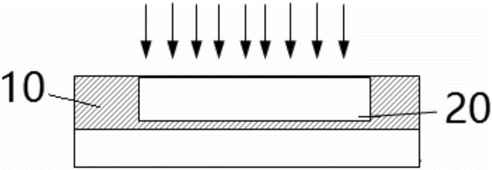
[0033] The first step: perform well region ion implantation and channel ion implantation (such as figure 2 Shown by the arrow) to form the device region 20;

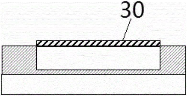
[0034] The second step: forming a gate oxide layer 30 on the top of the device region 20;

[0035] Step 3: forming a gate structure 40 including a gate spacer on the gate oxide layer 30 b...


PUM


Abstract

The invention provides a method for improving an ESD protective capability of an SOI NMOS device and the SOI NMOS device. The method for improving the ESD protective capability of the SOI NMOS device comprises: carrying out well region ion injection and channel ion injection in a silicon top layer of SOI to form a device area; forming a gate oxide layer at the top of the device area; forming a gate structure containing gate side walls on the gate oxide layer through deposition and etching; arranging a photoresist layer on the exposed silicon top layer surface and device area surface and partially removing the photoresist layer from the device area surface so as to partially expose the device area surface; carrying out partial inclined injection by using the photoresist layer to form a partial ESD ion injection area in the device area; and respectively forming a drain electrode and a source electrode in the device area on two sides of the gate structure.

Description

technical field [0001] The present invention relates to the field of semiconductor manufacturing, more specifically, the present invention relates to a kind of method that improves SOI (Silicon-On-Insulator, silicon on insulating substrate or silicon on insulator) NMOS device electrostatic discharge (Electro Static Discharge, ESD) protection ability Methods and SOI NMOS devices. Background technique [0002] As semiconductor device technology continues to enter submicron and deep submicron, the reliability of electrostatic discharge (ESD) protection devices is becoming more and more important. In order to overcome the problem of the decrease of electrostatic discharge protection ability caused by lightly doped drain (Lightly Doped Drain, LDD) structure, electrostatic discharge ion implantation (ESD implant) technology is used to improve the electrostatic discharge protection ability of the device. The method is as follows: figure 1 As shown, electrostatic discharge injectio...

Claims


Application Information

Patent Timeline
Patent Type & Authority Applications(China)
IPC IPC(8): H01L23/60H01L29/06H01L21/336H01L29/78
CPCH01L23/60H01L29/0623H01L29/66568H01L29/78
Inventor 颜丙勇杜宏亮
Owner SHANGHAI HUALI MICROELECTRONICS CORP
Why Eureka
Try Eureka