Low capacitance transient voltage suppressor (TVS) with reduced clamping voltage

a transient voltage suppressor and low capacitance technology, applied in the field of integrated circuits, can solve the problems of unexpected and uncontrollable high voltage hitting the circuit, and achieve the effects of improving the clamping performance of an n+ source, low capacitance, and easy integration of steering diodes

Active Publication Date: 2014-04-15
ALPHA & OMEGA SEMICON INC
View PDF27 Cites 26 Cited by
  • Summary
  • Abstract
  • Description
  • Claims
  • Application Information

AI Technical Summary

Benefits of technology

[0022]Additionally, an isolation layer (not shown) may be formed above the second epitaxial layer 209 with openings formed therein to provide for metal contacts. A Vcc pad (not shown) may make contact to the second source region 219′ above the Zener diode through an opening in the isolation layer. An n-type sinker region 217 may be formed between the second source region 219′ and the n+ buried layer 205 to allow the Zener diode to form a connection at the top surface of the device 200. In reverse mode, the n-type sinker region 217 acts as part of a PN junction that can be used to improve the clamping performance of an N+ source to the substrate 201 both in positive and negative mode. An I / O pad (not shown) may make contact to the p+ implant region 221 (i.e., anode of high-side steering diode) through another opening in the isolation layer. Additionally, a second I / O pad (not shown) may make contact to the third source region 219″ (i.e., cathode of low-side steering diode) through yet another opening in the isolation layer.
[0023]As illustrated, the conventional TVS 200 operates and functions as described above with respect to the circuit diagram in FIG. 1. This conventional TVS 200 exhibits several desirable device characteristics. For one, the conventional TVS 200 is built on a p-type substrate 201, which allows for the substrate to act as ground, facilitating easier integration of the steering diodes HSD, LSD and the Zener diode. Additionally, the conventional TVS 200 exhibits low capacitance due to light doping of the second epitaxial layer 209 as well as a small device package size attributed to vertical integration of the steering diodes and Zener diode.
[0029]The first epitaxial layer 303 is a lightly doped n- layer. This first epitaxial layer 303 may be doped with phosphorous having a concentration on the order of 2×10¹⁶ / cm3. The second epitaxial layer 309 is a very lightly doped p− layer. This second epitaxial layer 309 may be doped with Boron, having a minimal doping concentration on the order of 1014 / cm3 or lower. Because the doping concentration of the second epitaxial layer 309 contributes significantly to the capacitance of both the high-side steering diode HSD and low-side steering diode LSD it is desirable to set the doping concentration of this layer 309 as low as possible. The capacitances of the steering diodes HSD, LSD will contribute significantly to the overall capacitance of the TVS 300 because the steering diodes HSD, LSD are connected in parallel to the avalanche diode. Thus, the capacitances of the steering diodes HSD, LSD may be used to effectively lower the overall TVS 300 capacitance to a desired value regardless of the capacitance of the avalanche diode.
[0031]The avalanche diode (i.e., N-P-N structure) in the TVS 300 illustrated behaves differently than the Zener diode in the conventional TVS 200. Whereas the breakdown voltage behavior of the Zener diode in the conventional TVS 200 was solely dependent on the doping concentration of the p+ implant region and limited by reverse leakage current issues, the breakdown voltage of the avalanche diode in the invented TVS 300 lends itself to more flexibility. The breakdown voltage of the avalanche diode is dependent on two different factors: the breakdown voltage of the P-N junction (i.e., junction between P+ implant layer 307 and N+ buried layer 305) and the gain of the N-P-N structure. The breakdown voltage of the avalanche diode is directly proportional to the breakdown voltage of the P-N junction and inversely proportional to the gain of the N-P-N structure. As such, the doping concentration of the p+ implant layer 307 may remain at a level necessary to prevent reverse leakage current, while the gain of the N-P-N is adjusted in order to obtain a desired TVS breakdown voltage. The gain of the N-P-N structure is dependent on the thickness of the base, which in this case is the p+ implant layer 307. By decreasing the thickness of this p+ implant layer 307, the breakdown voltage of the TVS may also be effectively decreased. Thus, the breakdown voltage of the TVS may be reduced below 6V to support a wider range of applications by decreasing the thickness of the p+ implant layer 307. Because the clamping voltage of the TVS is heavily dependent on the breakdown voltage, it too may also be effectively reduced by adjusting the gain of the avalanche diode (i.e., reducing the thickness of p+ implant layer 307).
[0040]The TVS 300′ in FIG. 3B retains the same structure as the TVS 300 in FIG. 3A, except for the addition of a polysilicon layer 315 within each isolation trench 311, 311′, 311″. Each isolation trench 311, 311′, 311″ is first filled with a thin layer of oxide 313 and the remainder is subsequently filled with polysilicon 315. The process of filling a trench 311, 311′, 311″ with polysilicon 315 rather than oxide greatly simplifies the manufacturing process. Lining the trenches with oxide and filling them with polysilicon is easier than filling the trenches with oxide and avoids a complex process that tends to introduce high stress in the resulting structure. The isolation trenches 311, 311′, 311″ continue to isolate the low-side steering diode LSD from the high-side steering diode HSD integrated with the avalanche diode. This TVS device 300′ continues to operate and function as described above with respect to the circuit diagram in FIG. 1.

Problems solved by technology

However, in situations such as electrostatic discharge (ESD), electrical fast transients and lightning, an unexpected and an uncontrollable high voltage may accidentally strike onto the circuit.

Method used


Image

  • Low capacitance transient voltage suppressor (TVS) with reduced clamping voltage
  • Low capacitance transient voltage suppressor (TVS) with reduced clamping voltage
  • Low capacitance transient voltage suppressor (TVS) with reduced clamping voltage

Examples


Embodiment Construction

Introduction

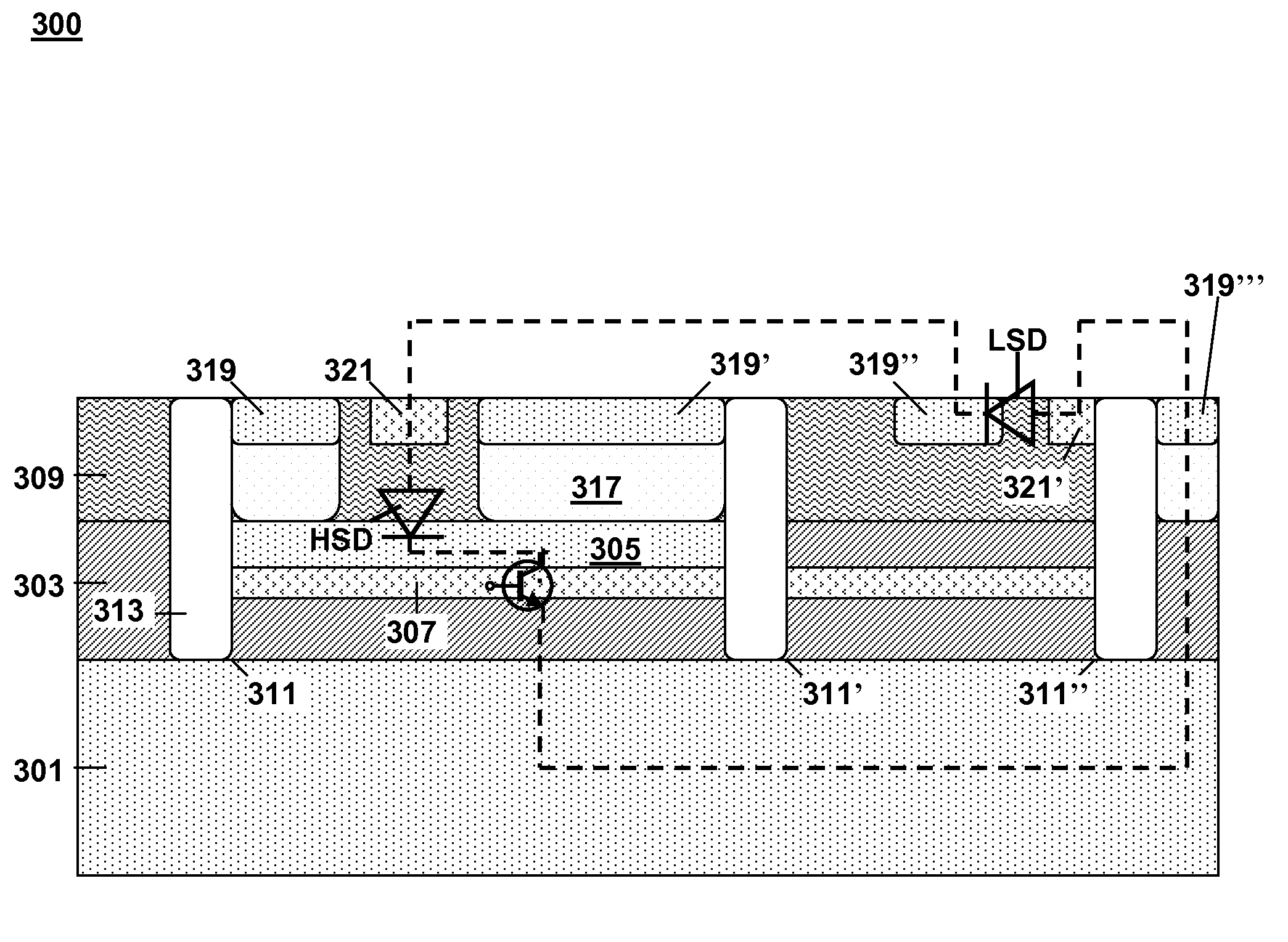
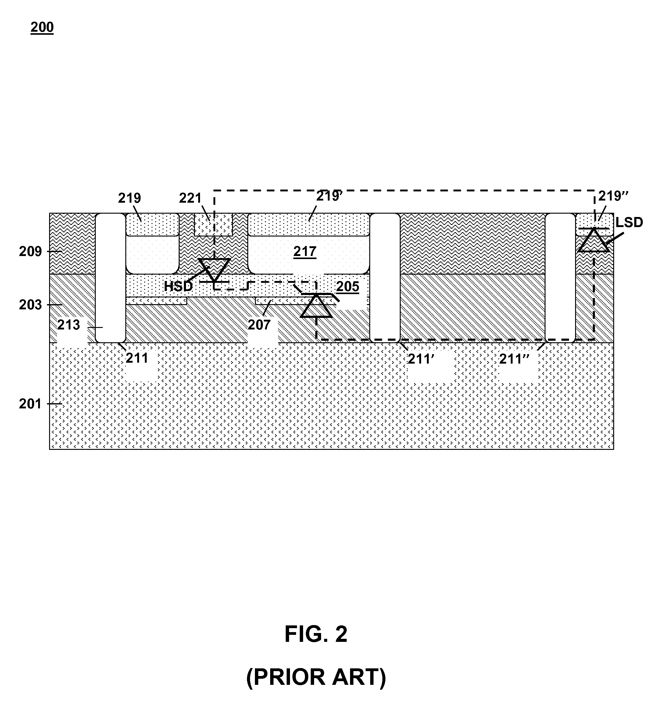
[0016]FIG. 2 is a cross-sectional schematic diagram illustrating a conventional transient voltage suppressor (TVS) device 200 in accordance with the prior art. This conventional TVS 200 behaves in accordance with the TVS 100 described above in the circuit diagram of FIG. 1.

[0017]The TVS 200 is formed on a heavily doped p+ semiconductor substrate 201 which supports a first epitaxial layer 203 and a second epitaxial layer 209. The first epitaxial layer 203 is a lightly doped p− layer. This first epitaxial layer 203 may be doped with Boron having a concentration on the order of 1015 / cm3. The second epitaxial layer 209 is a very lightly doped p− layer. This second epitaxial layer 209 may also be doped with Boron, having an even lower doping concentration on the order of 1014 / cm3 or lower. Because the doping concentration of the second epitaxial layer 209 contributes significantly to the capacitance of both the high-side steering diode HSD and low-side steering diode LSD it i...


PUM


Abstract

A low capacitance transient voltage suppressor with reduced clamping voltage includes an n+ type substrate, a first epitaxial layer on the substrate, a buried layer formed within the first epitaxial layer, a second epitaxial layer on the first epitaxial layer, and an implant layer formed within the first epitaxial layer below the buried layer. The implant layer extends beyond the buried layer. A first trench is at an edge of the buried layer and an edge of the implant layer. A second trench is at another edge of the buried layer and extends into the implant layer. A third trench is at another edge of the implant layer. Each trench is lined with a dielectric layer. A set of source regions is formed within a top surface of the second epitaxial layer. The trenches and source regions alternate. A pair of implant regions is formed in the second epitaxial layer.

Description

FIELD OF INVENTION[0001]This invention relates to integrated circuits and more specifically to a transient voltage suppressor (TVS).BACKGROUND OF INVENTION[0002]Transient voltage suppressors (TVS) are devices used to protect integrated circuits from damages caused by over voltage imposed onto the integrated circuit. An integrated circuit is designed to operate over a normal range of voltages. However, in situations such as electrostatic discharge (ESD), electrical fast transients and lightning, an unexpected and an uncontrollable high voltage may accidentally strike onto the circuit. The TVS devices are required to provide protection to circumvent the damages that are likely to occur to the integrated circuits when such over voltage conditions occur. As an increasing number of devices are implemented with integrated circuits that are vulnerable to over voltage damages, demands for TVS protection are also increased. Exemplary applications of TVS can be found in USB power and data lin...

Claims


Application Information

Patent Timeline
Patent Type & Authority Patents(United States)
IPC IPC(8): H01L29/66H01L29/06
CPCH01L27/0255H01L29/66113H01L21/76224H01L21/822H01L21/265H01L27/0248
Inventor GUAN, LINGPENGBOBDE, MADHURBHALLA, ANUPHU, JUNENG, WAYNE F.
Owner ALPHA & OMEGA SEMICON INC
Why Eureka
Try Eureka