Silicon carbide power device having protective diode

a technology of silicon carbide and power device, which is applied in the direction of semiconductor devices, semiconductor device details, electrical apparatus, etc., can solve the problems of static electricity, gate is not insulated from the channel region, and the proposed device is relatively easily destroyed

Inactive Publication Date: 2005-02-15
DENSO CORP
View PDF12 Cites 29 Cited by
  • Summary
  • Abstract
  • Description
  • Claims
  • Application Information

AI Technical Summary

Benefits of technology

In the present invention, a silicon carbide power device includes a protective diode, which is a Zener or PN junction diode, in addition to a JFET to prevent the JFET from being destroyed and to protect a circuit that controls a gate of the JFET. Each of the JFET and the protective diode includes a PN junction formed with layers that are substantially made of silicon carbide. The PN junction of the protective diode has a breakdown voltage lower than the PN junction of the JFET to protect the JFET.

Problems solved by technology

However, when the proposed device is used as a switching device such as an inverter for controlling a motor, there is the following problem in the proposed device.
The proposed device is relatively readily destroyed by static electricity generated in the manufacturing process, by overheat due to an excessive current caused when the motor is locked, or by surge energy due to counter electromotive force generated when the inverter controls the motor.
In addition, the proposed device includes a gate and a channel, and the gate is not insulated from the channel region by an oxide film as is in a MOSFET.
Therefore, if an avalanche breakdown is caused at a PN junction in the proposed device, the current generated by the avalanche breakdown flows from the gate into a circuit that controls the gate to destroy the circuit.

Method used


Image

  • Silicon carbide power device having protective diode
  • Silicon carbide power device having protective diode
  • Silicon carbide power device having protective diode

Examples


first embodiment

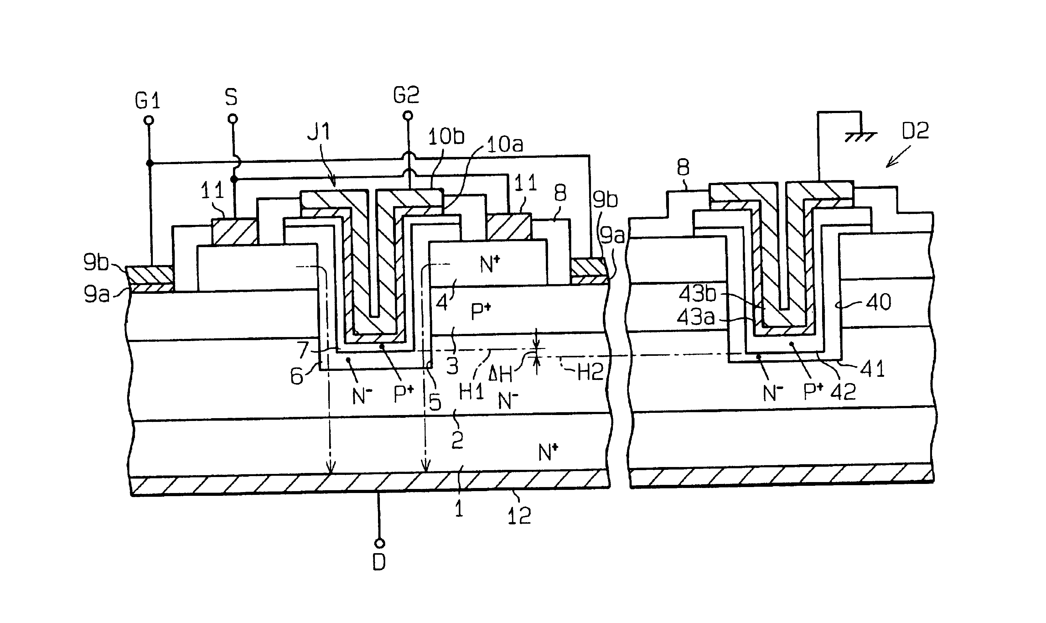
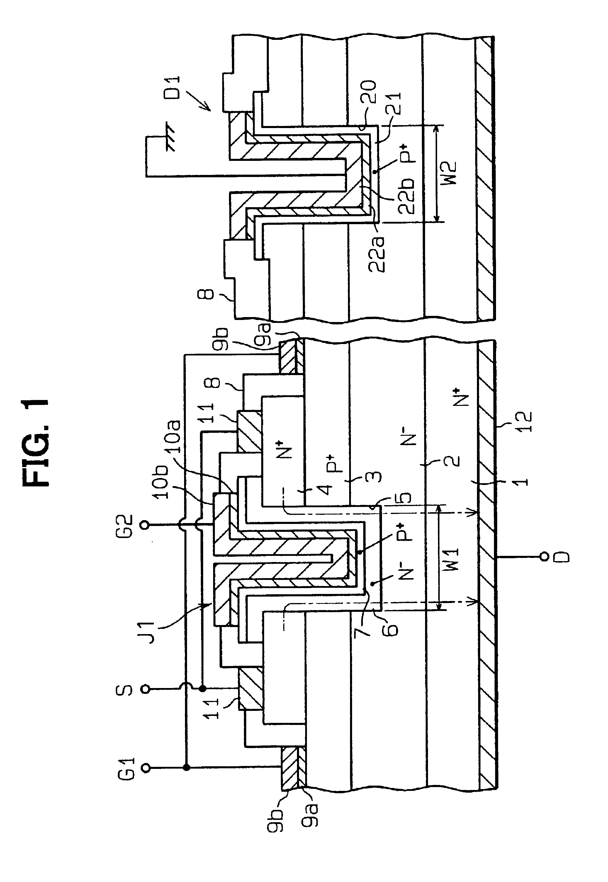
As shown in FIG. 1, a silicon carbide power device according to the first embodiment includes a JFET J1 as a silicon carbide power transistor and a protective diode D1, which is a Zener or PN junction diode, as a surge absorber. The silicon carbide power device includes an n+-type substrate 1, which has a first conduction type, an n−-type drift layer 2, which has the first conduction type, a p+-type first gate layer 3 (first JFET impurity layer), which has a second conduction type, and an n+-type source layer 4, which has the first conduction type. The substrate 1 and the layers 2, 3, 4 are substantially made of silicon carbide (SiC). The substrate 1 has a front surface and a back surface, which is opposite from the front surface. The layers 2, 3, 4 are sequentially layered in the above order on the front surface of the substrate 1. The impurity concentration of the n−-type drift layer 2 is lower than those of the n+-type substrate 1 and the n+-type source layer 4.

In the JFET J1, a ...

second embodiment

As shown in FIG. 9, a silicon carbide power device according to the second embodiment includes a JFET J1 and a protective diode D2, which is a Zener or PN junction diode different in structure from the protective diode D1 of the silicon carbide power device in FIG. 1, as a surge absorber.

In the protective diode D2, a second trench 40 extends from the upper surface of the n+-type source layer 4 to the n−-type drift layer 2 through the p+-type first gate layer 3. An n−-type impurity layer 41 (first diode impurity layer) and a p+-type impurity layer 42 (second diode impurity layer), which are substantially made of SiC, are located on the surface defining the trench 40. An electrode, which includes an ohmic contact electrode 43a and a wiring electrode 43b, is located on the p+-type impurity layer 42 and is grounded. As viewed in FIG. 9, there is a difference ΔH between the bottom level H1 of the p+-type second gate layer 7 and the bottom level H2 of the p+-type impurity layer 42. The p+...

third embodiment

As shown in FIG. 16, a silicon carbide power device according to the second embodiment includes two JFETs J1 as silicon carbide power transistors and a protective diode D3, which is a Zener or PN junction diode different in structure from the protective diodes D1, D2 of the silicon carbide power devices in FIGS. 1 and 9, as a surge absorber. The protective diode D3 includes a p+-type region 50, which is located in the upper surface of the n−-type drift layer 2, and an electrode, which includes an ohmic contact electrode 51a and a wiring electrode 51b, as viewed in FIG. 16. The electrode of the protective diode D3 is located on the upper surface of the p+-type first gate layer 3. The electrode of the protective diode D3 is in ohmic contact with the p+-type first gate layer 3 and is grounded.

As viewed in FIG. 16, there is a difference ΔH in distance between the bottom level H3 of each p+-type second gate layer 7 and the bottom level H4 of the p+-type region 50. Therefore, the p+-type ...


PUM


Abstract

A silicon carbide power device includes a junction field effect transistor and a protective diode, which is a Zener or PN junction diode. The PN junction of the protective diode has a breakdown voltage lower than the PN junction of the transistor. Another silicon carbide power device includes a protective diode, which is a Schottky diode. The Schottky diode has a breakdown voltage lower than the PN junction of the transistor by adjusting Schottky barrier height or the depletion layer formed in the semiconductor included in the Schottky diode. Another silicon carbide power device includes three protective diodes, which are Zener diodes. Two of the protective diodes are used to clamp the voltages applied to the gate and the drain of the transistor due to surge energy and used to release the surge energy. The last diode is a thermo-sensitive diode, with which the temperature of the JFET is measured.

Description

CROSS REFERENCE TO RELATED APPLICATIONThis application is based on and incorporates herein by reference Japanese Patent Applications No. 2001-259661 filed on Aug. 29, 2001 and No. 2001-259996 filed on Aug. 29, 2001.BACKGROUND OF THE INVENTIONThe present invention relates to a silicon carbide power device having a protective diode and the method for manufacturing the power device.A silicon carbide power device including a junction field effect transistor (JFET) is proposed in JP-A-2000-312008. However, when the proposed device is used as a switching device such as an inverter for controlling a motor, there is the following problem in the proposed device. The proposed device is relatively readily destroyed by static electricity generated in the manufacturing process, by overheat due to an excessive current caused when the motor is locked, or by surge energy due to counter electromotive force generated when the inverter controls the motor. In addition, the proposed device includes a ga...

Claims


Application Information

Patent Timeline
Patent Type & Authority Patents(United States)
IPC IPC(8): H01L21/02H01L29/66H01L21/04H01L29/866H01L29/808H01L29/872H01L29/861H01L29/24H01L29/02
CPCH01L29/66068H01L29/66992H01L29/872H01L29/861H01L29/866H01L29/8083H01L29/1608
Inventor KUMAR, RAJESHNAKAMURA, HIROKIYAMAMOTO, TSUYOSHIMORISHITA, TOSHIYUKI
Owner DENSO CORP
Why Eureka
Try Eureka