Semiconductror device and manufacturing method thereof

a technology of semiconductors and manufacturing methods, applied in semiconductor devices, basic electric elements, electrical equipment, etc., can solve problems such as reducing breakdown voltage, and achieve the effect of preventing a reduction of breakdown voltag

Active Publication Date: 2009-04-16
LAPIS SEMICON CO LTD
View PDF3 Cites 28 Cited by
  • Summary
  • Abstract
  • Description
  • Claims
  • Application Information

AI Technical Summary

Benefits of technology

[0004]The present invention has been made in view of the foregoing points. It is an object of the present invention to provide a semiconductor device capable of preventing a reduction in breakdown voltage without depletion layers spread from adjoining vertical field effect transistors being connected to one another.

Problems solved by technology

It is feared that no depletion layers are connected to each other particularly in a region increasing with distance from P-type base regions, such as a region surrounded by at least three DMOS transistors adjacent to one another, thus causing a reduction in breakdown voltage.

Method used


Image

  • Semiconductror device and manufacturing method thereof
  • Semiconductror device and manufacturing method thereof
  • Semiconductror device and manufacturing method thereof

Examples


Embodiment Construction

[0023]Preferred embodiments of the present invention will hereinafter be described in detail with reference to the accompanying drawings.

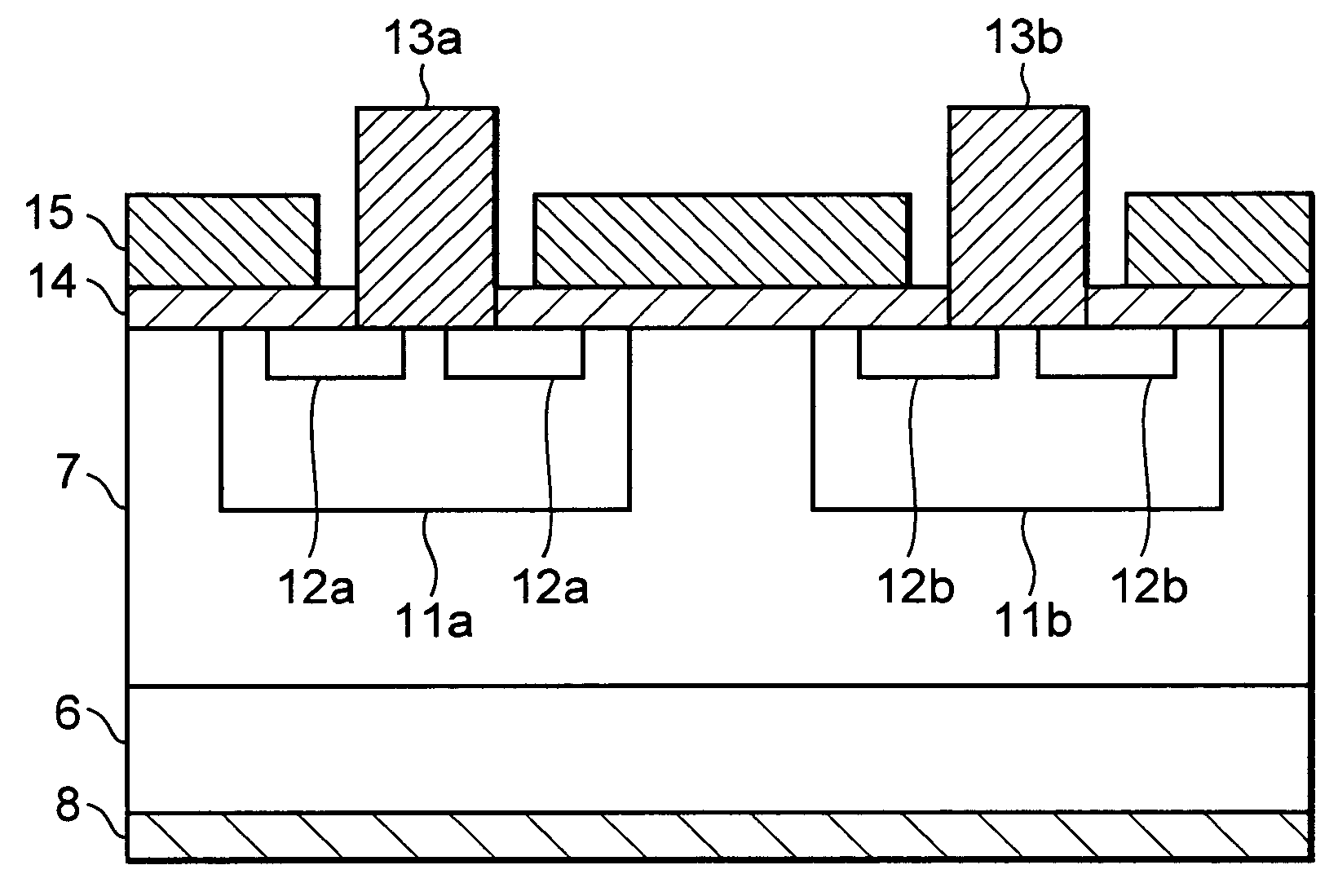
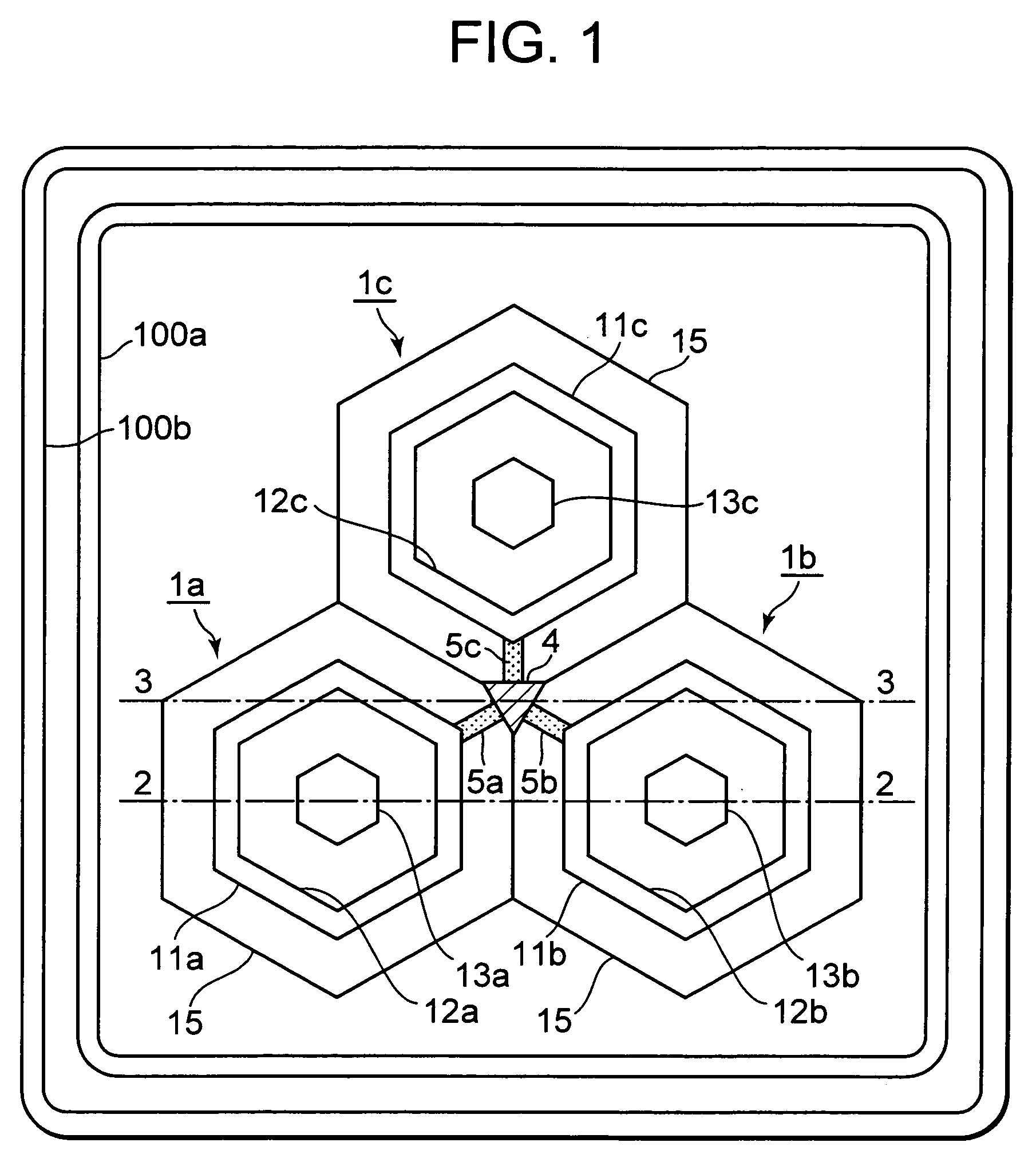
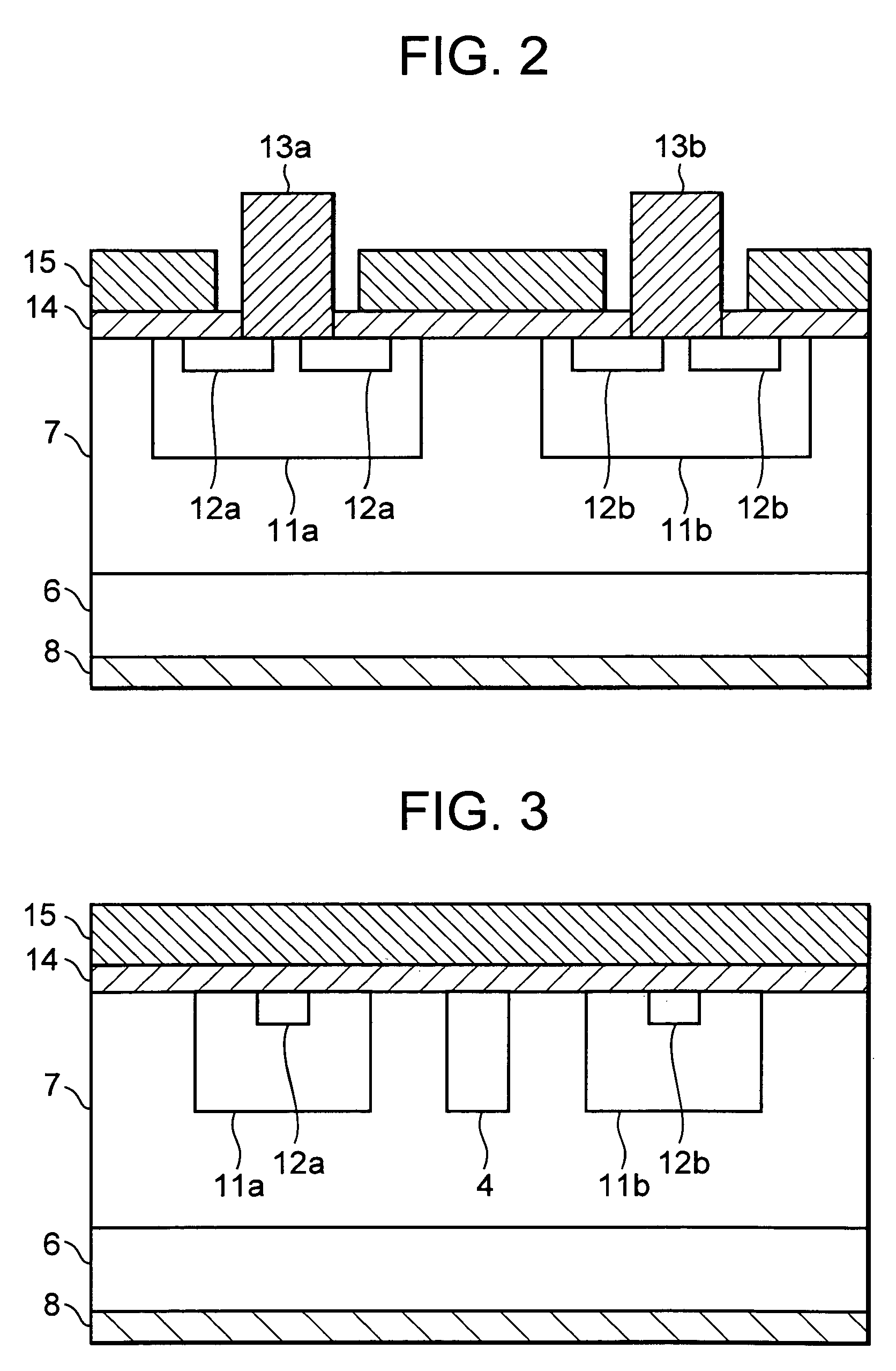
[0024]FIG. 1 is a plan view showing a structure of one embodiment illustrative of a semiconductor device according to the present invention. The semiconductor device comprises three field effect transistors 1a through 1c. FLRs (Field Limiting Rings) 100a and 100b are formed so as to surround the field effect transistors 1a through 1c. Planar shapes of a base region 11a, a source region 12 and a source electrode 13a of the field effect transistor 1a are respectively hexagonal. Incidentally, other field effect transistors 1b and 1c respectively also take planar shapes similar to the field effect transistor 1a. An intermediate region 4 is formed in the center of a region surround by the three field effect transistors 1a through 1c. A connection region 5a is formed so as to contact the intermediate region 4 and the base region 11a of the field effect t...


PUM


Abstract

A semiconductor device includes field effect transistors, each having a semiconductor layer formed on a major surface of a semiconductor substrate, a base region formed in a surface layer portion of a semiconductor layer, a source region formed in a surface layer portion of the base region, a source electrode formed on the base region and the source region, a gate electrode formed on the semiconductor layer and the base region via a gate insulating film interposed therebetween, and a drain electrode formed on a back surface of the semiconductor substrate, and which are placed side by side. A columnar intermediate region is formed in its corresponding predetermined region of the surface layer portion of the semiconductor layer placed below each gate electrode. Connection regions are formed in the surface layer portion of the semiconductor layer to contact the intermediate region and the base regions.

Description

BACKGROUND OF THE INVENTION[0001]The present invention relates to a semiconductor device which includes a plurality of vertical field effect transistors and wherein the field effect transistors are provided side by side with one another, and a manufacturing method thereof.[0002]DMOS transistors each corresponding to a vertical field effect transistor have been known as semiconductor elements each of which enables large current to flow therethrough and is capable of being operated at a high voltage. The DMOS transistor allows current to flow between a source electrode formed on a major surface of a semiconductor substrate and a drain electrode formed on a back surface of the semiconductor substrate. A P-type base region is formed in its corresponding surface layer portion on the major surface side of the N-type semiconductor substrate, and an N-type source region is formed in its corresponding surface layer portion of the P-type base region. A source electrode is formed so as to cont...

Claims


Application Information

Patent Timeline
Patent Type & Authority Applications(United States)
IPC IPC(8): H01L21/336H01L29/78
CPCH01L29/0619H01L29/0696H01L29/7802H01L29/66068H01L29/1608
Inventor YAMANOBE, TOMOMI
Owner LAPIS SEMICON CO LTD
Why Eureka
Try Eureka