Semiconductor device and method of manufacturing semiconductor device

a semiconductor and semiconductor technology, applied in the direction of semiconductor devices, basic electric elements, electrical appliances, etc., can solve the problems of increasing on-resistance, reducing the withstand capability of the device, and manufacturing extremely difficult, so as to reduce the on-resistance, increase the on-resistance, and manufacture extremely difficult

Active Publication Date: 2017-05-18
FUJI ELECTRIC CO LTD
View PDF2 Cites 29 Cited by
  • Summary
  • Abstract
  • Description
  • Claims
  • Application Information

AI Technical Summary

Benefits of technology

[0010]However, when the p-n junction is formed using the technology disclosed in Patent Document 1, a sufficient breakdown voltage cannot be achieved unless the p-n junction is formed at a position deeper than the bottom of the trench or a position near the trench, which makes manufacturing extremely difficult. Moreover, when a p-type region is formed using the technology disclosed in Patent Document 2, the gate insulating film on the sidewalls of the trench tends to get subjected to strong electric fields, and the current path becomes narrow in the ON state, which increases the on-resistance. Furthermore, when both a deep p-type structure is formed at a position away from the trench and a p-type region is formed at the bottom of the trench using the technology disclosed in Patent Document 3, the width of the p-type region at the bottom of the trench is made narrower than the width of the trench in order to reduce the on-resist...

Problems solved by technology

However, when the p-n junction is formed using the technology disclosed in Patent Document 1, a sufficient breakdown voltage cannot be achieved unless the p-n junction is formed at a position deeper than the bottom of the trench or a position near the trench, which makes manufacturing extremely difficult.
Moreover, when a p-type region is formed using the technology ...

Method used


Image

  • Semiconductor device and method of manufacturing semiconductor device
  • Semiconductor device and method of manufacturing semiconductor device
  • Semiconductor device and method of manufacturing semiconductor device

Examples


embodiment 1

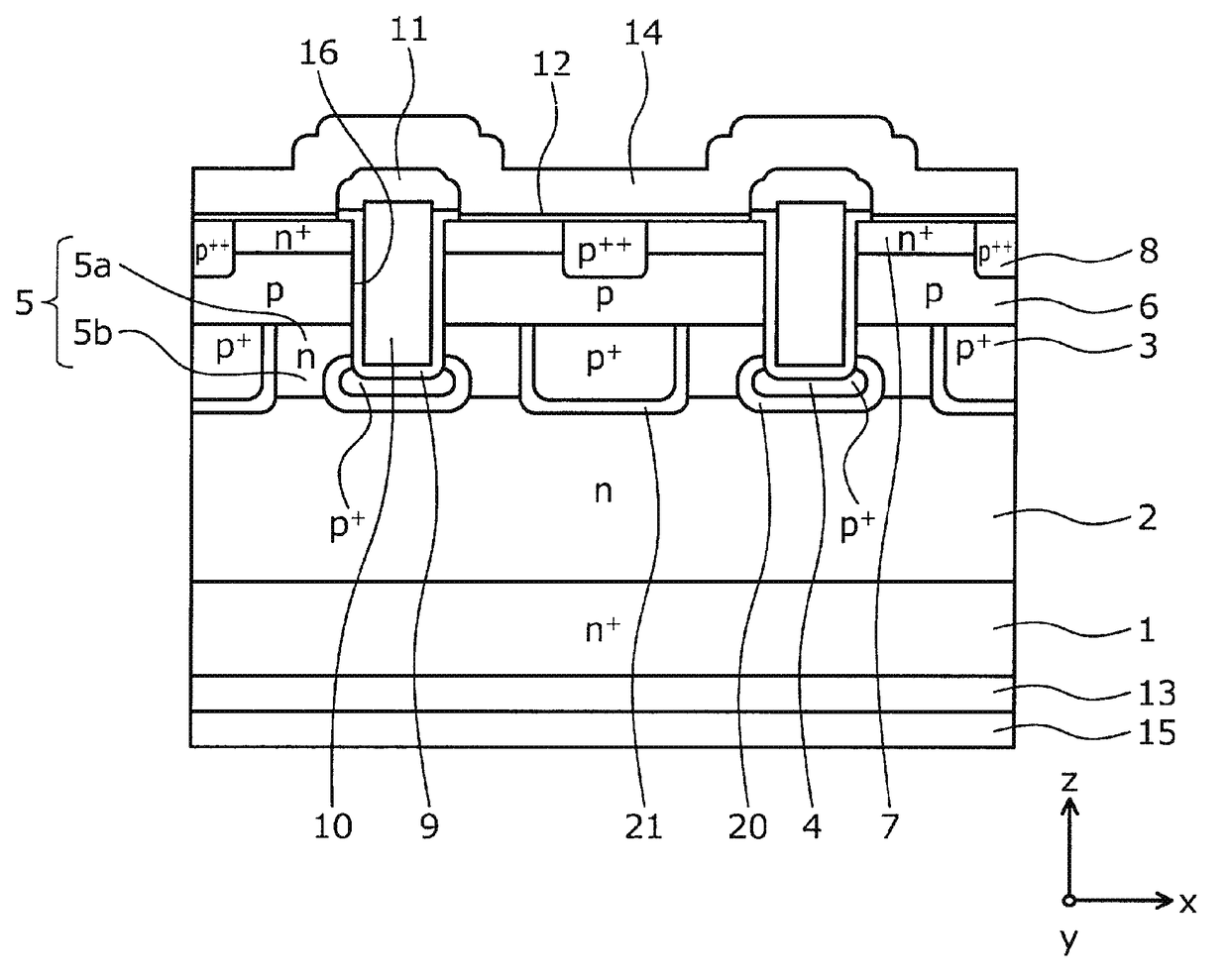
[0038]The semiconductor device according to one aspect of the present invention is formed using a wide-bandgap semiconductor. In the present embodiment, a silicon carbide semiconductor device manufactured using silicon carbide (SiC) as the wide-bandgap semiconductor, for example, will be described using a MOSFET as an example. FIG. 1 is a cross-sectional view illustrating a configuration of the silicon carbide semiconductor device according to Embodiment 1.

[0039]As illustrated in FIG. 1, in the silicon carbide semiconductor device according to the present embodiment, an n-type silicon carbide epitaxial layer (a first wide-bandgap semiconductor layer of a first conductivity type) 2 is deposited onto a first principal surface (the front surface; here, the (0001) plane (Si plane), for example) of an n+ silicon carbide substrate (a wide-bandgap semiconductor substrate of the first conductivity type) 1.

[0040]The n+ silicon carbide substrate 1 is a monocrystalline silicon carbide substrat...

working example

[0070]FIG. 8 is a graph comparing the current-voltage characteristics of the silicon carbide semiconductor device according to Embodiment 1 and the current-voltage characteristics of a conventional silicon carbide semiconductor device. FIG. 9 is a cross-sectional view illustrating a configuration of the conventional silicon carbide semiconductor device. The conventional silicon carbide semiconductor device is a vertical trench-gate MOSFET in which the first n-type regions 20 and the second n-type regions 21 of the silicon carbide semiconductor device according to Embodiment 1 are removed.

[0071]FIG. 8 is a graph in which the current that flows through the drain electrode 13 and the source electrode 12 in the ON state is plotted against the voltage between the drain electrode 13 and the source electrode 12. In FIG. 8, the horizontal axis is the voltage, and the vertical axis is the current. The line labeled “Working Example” represents the current-voltage characteristics of the silico...

embodiment 2

[0077]FIG. 10 is a cross-sectional view illustrating a configuration of a silicon carbide semiconductor device according to Embodiment 2. As illustrated in FIG. 10, the silicon carbide semiconductor device according to Embodiment 2 is a structure in which third p-type regions 3c are formed contacting the bottom ends (drain side ends) of first p+ base regions 3 in an n-type silicon carbide epitaxial layer 2 and in which fourth n-type regions 21 surround the third p-type regions 3c. Together, the third p-type regions 3c, a p-type base layer 6, and the first p+ base regions 3 function as base regions.

[0078]The thickness of the third p-type regions 3c may be approximately 0.1 μm to 0.5 μm, for example. The width of the third p-type regions 3c is less than the width of the first p+ base regions 3 and may be 0.1 μm or more less than the width of the first p+ base regions 3, for example. Moreover, the third p-type regions 3c may be formed continuously and with the same thickness running in...


PUM


Abstract

Trenches and n+ high impurity concentration regions are formed in a first principal surface side of a silicon carbide semiconductor substrate. In the n+ high impurity concentration regions, third n-type regions that respectively surround first p+ base regions contacting a p-type base layer and have a higher impurity concentration than the n+ high impurity concentration regions, as well as fourth n-type regions that respectively surround second p+ base regions formed at the bottoms of the trenches and also have a higher impurity concentration than the n+ high impurity concentration regions, are formed.

Description

BACKGROUND OF THE INVENTION[0001]Technical Field[0002]The present invention relates to a semiconductor device and a method of manufacturing the semiconductor device.[0003]Background Art[0004]In conventional power semiconductor devices, vertical metal-oxide-semiconductor field-effect transistors (MOSFETs) that have a trench structure are manufactured to reduce the on-resistance of the device. In vertical MOSFETs, a trench structure in which a channel is formed orthogonal to the substrate surface makes it possible to achieve a higher cell density per unit area than a planar structure in which a channel is formed parallel to the substrate surface. This makes it possible to increase the current density per unit area and is advantageous from a cost perspective.[0005]However, when a trench structure is formed in a vertical MOSFET, the inner walls of the trench structure are entirely covered by a gate insulating film so that the channel can be formed in the vertical direction, and the port...

Claims


Application Information

Patent Timeline
IPC IPC(8): H01L29/78H01L29/36H01L29/08H01L21/02H01L29/423H01L29/16H01L29/66H01L29/10H01L29/417
CPCH01L29/7813H01L29/1079H01L29/36H01L29/0865H01L29/41741H01L29/4236H01L21/02634H01L29/7827H01L29/66068H01L29/66666H01L29/66734H01L21/02529H01L21/02378H01L29/1608H01L29/0623H01L29/0878H01L29/1095H01L29/0882H01L29/0886
Inventor HOSHI, YASUYUKI
Owner FUJI ELECTRIC CO LTD
Why Eureka
Try Eureka