Switching regulator control circuit

A switching voltage regulator and control circuit technology, applied in the direction of control/regulation systems, instruments, electrical components, etc., can solve problems such as deterioration of SW voltage regulators

Inactive Publication Date: 2005-02-09
SEIKO INSTR INC
View PDF1 Cites 17 Cited by
  • Summary
  • Abstract
  • Description
  • Claims
  • Application Information

AI Technical Summary

Problems solved by technology

[0008] However, the on-resistance and gate capacitance of the switching MOS transistor 11 have a trade-off relationship
That is, for example, when the efficiency at high loads dominates, there arises a problem that the efficiency of the SW regulator deteriorates to some extent at low loads within the range of PFM control operation (e.g., Can refer to JP2002-320379B)

Method used


Image

  • Switching regulator control circuit
  • Switching regulator control circuit

Examples


Embodiment Construction

[0014] Preferred embodiments of the present invention will be described below with reference to the accompanying drawings.

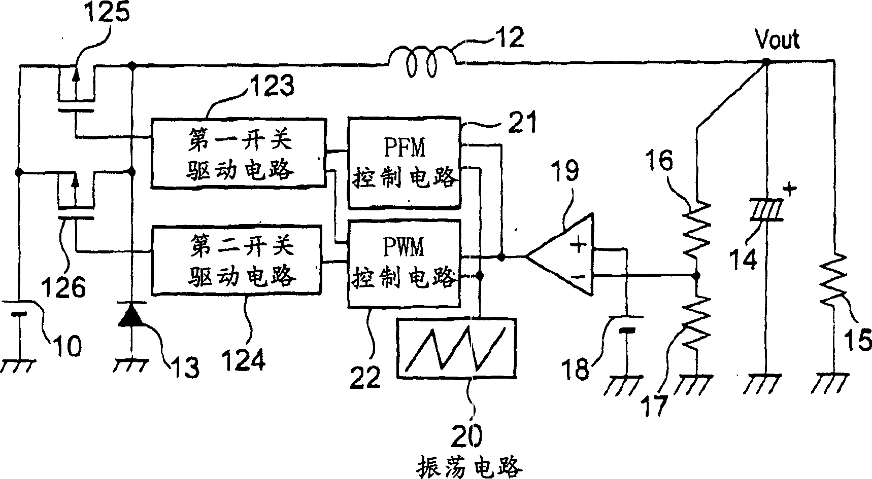
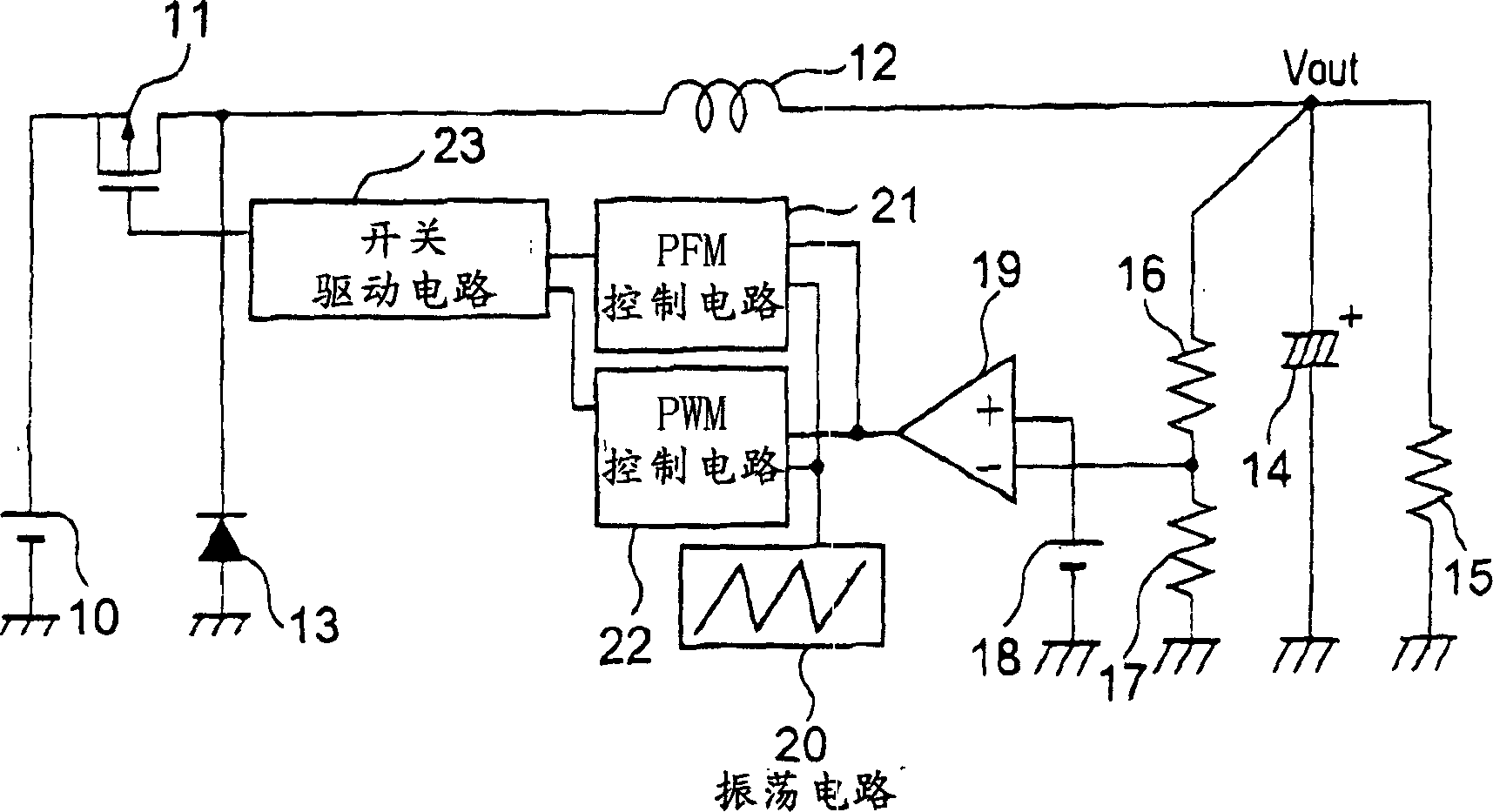
[0015] figure 1 A circuit block diagram showing a SW regulator control circuit according to the present invention. The reference voltage 18 , the voltage dividing resistor 16 , the voltage dividing resistor 17 , the error amplifier 19 , the oscillator circuit 20 , the PFM control circuit 21 and the PWM control circuit 22 are the same as the traditional SW regulator. The switch of the present SW regulator is characterized by having two transistors, a first switching MOS transistor 125 and a second switching MOS transistor 126, which are arranged in parallel and have high on-resistance and low gate capacitance.

[0016] In the case of a low load, the PFM control circuit 21 performs control such that the pulse width remains constant and the pulse frequency decreases to maintain the output voltage Vout. In this case, the first switch driving circuit 123 co...


PUM


Abstract

The present invention provides an SW regulator control circuit that is efficient in both of the cases where the load is heavy and where the load is light. Two switch MOS transistors are disposed as switching elements of the SW regulator in parallel which are large in an on-resistance and small in a gate capacity, and in the case where a load of the SW regulator is heavy, the two switch MOS transistors are driven in parallel to lessen the on-resistance whereas in the case where the load is light, one of the two switch MOS transistors is driven to lessen the gate capacity.

Description

technical field [0001] The present invention relates to a switching regulator (hereinafter referred to as "SW regulator") capable of improving efficiency at both high load and low load conditions. Background technique [0002] As shown in Figure 2, the traditional SW regulator control circuit includes: reference voltage 18, voltage divider resistors 16 and 17, error amplifier 19, oscillation circuit 20, pulse frequency modulation control circuit (hereinafter referred to as "PFM control circuit") 21 , a pulse width modulation control circuit (hereinafter referred to as “PWM control circuit”) 22 , a switch drive circuit 23 and a switch MOS transistor 11 . [0003] Assuming that the output voltage of the error amplifier 19 is Verr, the output voltage of the reference voltage 18 is Vref, and the voltage at the node between the voltage dividing resistor 16 and the voltage dividing resistor 17 is Va, if Vref>Va, then Verr rises, And if Vref<Va, then Verr decreases. [0004...

Claims


Application Information

Patent Timeline
Patent Type & Authority Applications(China)
IPC IPC(8): H02M3/155H02M3/158
CPCY02B70/16H02M3/1584H02M2001/0032Y02B70/10H02M1/0032H02M3/155
Inventor 森本茂之
Owner SEIKO INSTR INC
Why Eureka
Try Eureka