Semiconductor device with lifetime killers and method of manufacturing the same

a technology of semiconductor devices and lifetime killers, which is applied in the direction of semiconductor devices, diodes, electrical devices, etc., can solve the problems of increasing increasing the on-resistance, and increasing the probability of crystal defects, so as to facilitate current flow and increase the degree of variation in conductivity

Active Publication Date: 2018-08-16
FUJI ELECTRIC CO LTD
View PDF3 Cites 19 Cited by
  • Summary
  • Abstract
  • Description
  • Claims
  • Application Information

AI Technical Summary

Benefits of technology

[0012]Here, when a high voltage is applied to the source electrode 8 to drive the built-in p-n diode, current flows through the built-in p-n diode (as illustrated by A in FIG. 10, for example). At this time, in the SiC MOSFET, the forward voltage Vf of the built-in p-n diode satisfies Vf>Vth, and therefore in some cases current passes directly beneath the gate electrode 7 and flows through the p-n junction between the p-type base layer 3 and the n-type silicon carbide epitaxial layer 2 (as illustrated by B in FIG. 10, for example). This current causes carriers to be injected into the n+ silicon carbide substrate 1 and the n-type silicon carbide epitaxial layer 2, thereby making it easier for current to flow. This, in turn, increases the degree of variation in conductivity and makes crystal defects more likely to occur. These crystal defects cause ON-resistance to increase and also cause the threshold voltage Vth of the MOSFET as well as the forward voltage Vf of the built-in p-n diode to fluctuate.

Problems solved by technology

This, in turn, increases the degree of variation in conductivity and makes crystal defects more likely to occur.
These crystal defects cause ON-resistance to increase and also cause the threshold voltage Vth of the MOSFET as well as the forward voltage Vf of the built-in p-n diode to fluctuate.

Method used


Image

  • Semiconductor device with lifetime killers and method of manufacturing the same
  • Semiconductor device with lifetime killers and method of manufacturing the same
  • Semiconductor device with lifetime killers and method of manufacturing the same

Examples


embodiments

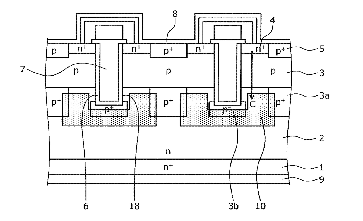
[0038]A semiconductor device according to the present embodiments is made using a wide-bandgap semiconductor which has a wider bandgap than silicon. In the embodiments, a silicon carbide semiconductor device manufactured using silicon carbide (SiC), for example, as the wide-bandgap semiconductor will be described using a vertical planar-gate MOSFET as an example. FIG. 1 is a cross-sectional view illustrating a configuration of the silicon carbide semiconductor device according to an embodiment.

[0039]As illustrated in FIG. 1, in the silicon carbide semiconductor device according to the embodiment, an n-type silicon carbide epitaxial layer (a first semiconductor layer of a first conductivity type) 2 is deposited onto a principal surface (the front surface) of an n+ silicon carbide substrate (a semiconductor substrate of the first conductivity type) 1.

[0040]The n+ silicon carbide substrate 1 is a monocrystalline silicon carbide substrate doped with nitrogen (N), for example. The n-type...


PUM


Abstract

A semiconductor device includes a semiconductor substrate, a first semiconductor layer of a first conductivity type, a second semiconductor layer of a second conductivity type, a first semiconductor region of the first conductivity type, a second semiconductor region of the second conductivity type, a gate insulating film, and a gate electrode. The semiconductor device further includes, in a region of the first semiconductor layer across or adjacent to a p-n junction therein that does not overlap the second semiconductor region in a plan view except lateral edges thereof, a lifetime killer region having lifetime killers implanted therein.

Description

BACKGROUND OF THE INVENTIONTechnical Field[0001]The present invention relates to a semiconductor device and a method of manufacturing the semiconductor device.Background Art[0002]Silicon (Si) has conventionally been used as the material for power semiconductor devices for controlling high voltages and high currents. There are various types of power semiconductor devices, such as bipolar transistors, insulated-gate bipolar transistors (IGBTs), and metal-oxide-semiconductor field-effect transistors (MOSFETs), and these devices are respectively used according to the purposes.[0003]For example, bipolar transistors and IGBTs offer higher current densities than MOSFETs and make it possible to work with higher currents but cannot be switched at high speeds. More specifically, bipolar transistors are limited to being used at switching frequencies on the order of several kHz, and IGBTs are limited to being used at switching frequencies on the order of several dozen kHz. Power MOSFETs, on the...

Claims


Application Information

Patent Timeline
Patent Type & Authority Applications(United States)
IPC IPC(8): H01L29/16H01L29/36H01L29/423H01L29/417H01L29/06H01L29/167H01L21/02H01L21/22H01L29/78H01L29/66H01L29/739
CPCH01L29/1608H01L29/36H01L29/42356H01L29/41741H01L29/0688H01L29/4236H01L29/167H01L21/02636H01L21/221H01L29/7813H01L29/7804H01L29/66734H01L29/66712H01L21/02529H01L29/66068H01L29/66333H01L29/66348H01L29/7395H01L29/7397H01L21/263H01L21/26506H01L29/0623H01L29/1095H01L29/7802
Inventor KUMADA, KEISHIROUHASHIZUME, YUICHIHOSHI, YASUYUKI
Owner FUJI ELECTRIC CO LTD
Why Eureka
Try Eureka