System and method for edge termination of super-junction (SJ) devices

a super-junction and power device technology, applied in the direction of semiconductor devices, basic electric elements, electrical equipment, etc., can solve the problems of significant higher electric fields present in wide bandgap semiconductor devices under

Active Publication Date: 2018-06-14
GENERAL ELECTRIC CO
View PDF0 Cites 17 Cited by
  • Summary
  • Abstract
  • Description
  • Claims
  • Application Information

AI Technical Summary

Benefits of technology

[0005]In an embodiment, a semiconductor super-junction (SJ) device includes a substrate layer having a first conductivity-type and one or more epitaxial (epi) layers disposed on the substrate layer and including a termination region disposed adjacent to an active region. The active region includes vertical charge-balance pillars of the first conductivity-type, each having a first width, and vertical charge-balance pillars of a second conductivity-type, each having a second width. The termination region includes a plurality of vertical pillars of the first and second conductivity-type, wherein, moving outward from the active region, a respective width of each successive vertical pillar of the plurality of vertical pillars is the same or smaller. The termination region also includes a plurality of compensated regions having a low doping concentration disposed directly between a first side of each vertical pillar of the first conductivity-type and a first side of each vertical pillar of the second conductivity-type, wherein, moving outward from the active region, a respective width of each successive compensated region of the plurality of compensated regions is the same or greater.

Problems solved by technology

However, there are also significantly higher electric fields present in wide bandgap semiconductors devices under reverse bias.

Method used


Image

  • System and method for edge termination of super-junction (SJ) devices
  • System and method for edge termination of super-junction (SJ) devices
  • System and method for edge termination of super-junction (SJ) devices

Examples


Embodiment Construction

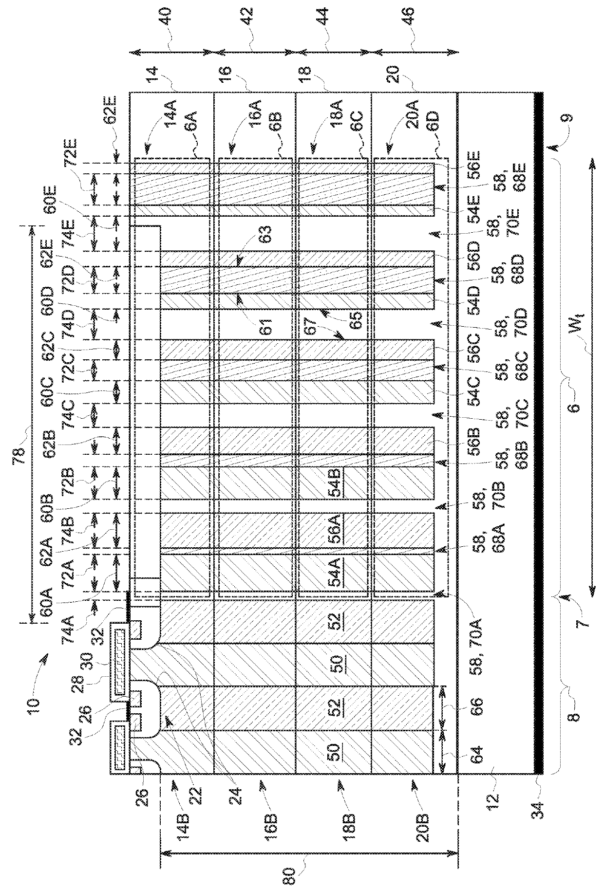
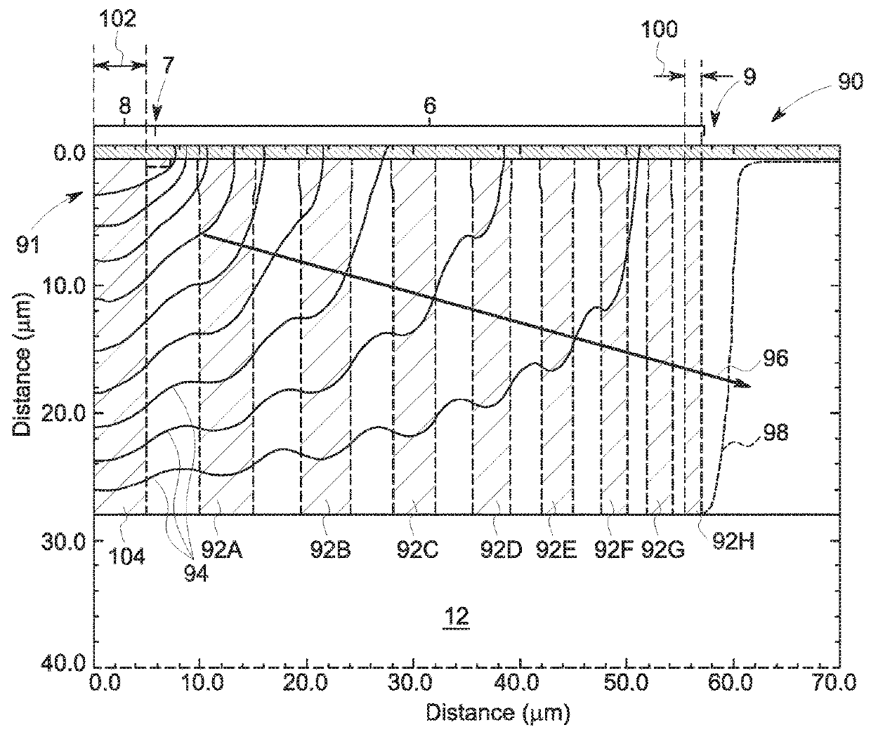
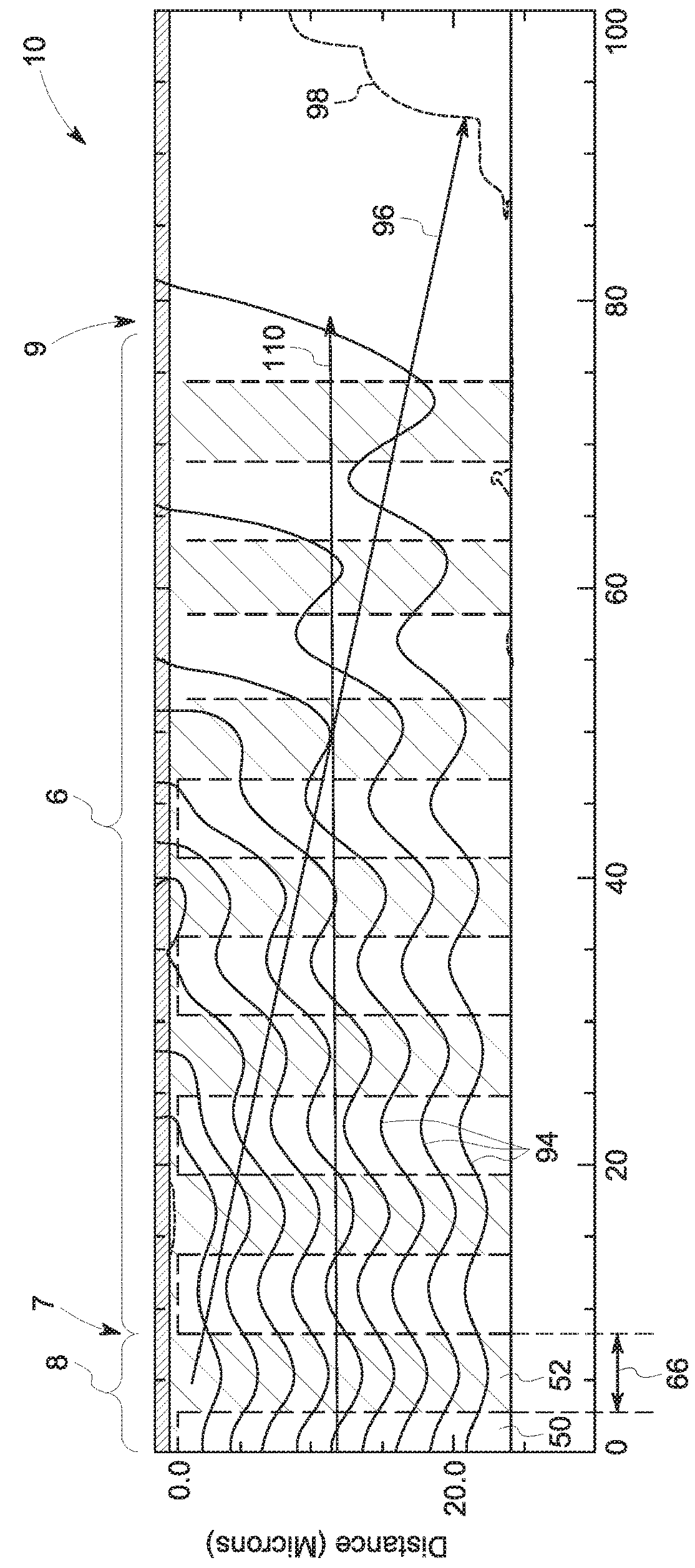
[0016]One or more specific embodiments will be described below. In an effort to provide a concise description of these embodiments, not all features of an actual implementation are described in the specification. It should be appreciated that in the development of any such actual implementation, as in any engineering or design project, numerous implementation-specific decisions must be made to achieve the developers' specific goals, such as compliance with system-related and business-related constraints, which may vary from one implementation to another. Moreover, it should be appreciated that such a development effort might be complex and time consuming, but would nevertheless be a routine undertaking of design, fabrication, and manufacture for those of ordinary skill having the benefit of this disclosure.

[0017]Unless defined otherwise, technical and scientific terms used herein have the same meaning as is commonly understood by one of ordinary skill in the art to which this disclo...


PUM


Abstract

The subject matter disclosed herein relates to super-junction (SJ) power devices and, more specifically, to edge termination techniques for SJ power devices. A semiconductor super-junction (SJ) device includes one or more epitaxial (epi) layers having a termination region disposed adjacent to an active region. The termination region includes a plurality of vertical pillars of a first and a second conductivity-type, wherein, moving outward from the active region, a respective width of each successive vertical pillar is the same or smaller. The termination region also includes a plurality of compensated regions having a low doping concentration disposed directly between a first side of each vertical pillar of the first conductivity-type and a first side of each vertical pillar of the second conductivity-type, wherein, moving outward from the active region, a respective width of each successive compensated region is the same or greater.

Description

BACKGROUND[0001]The subject matter disclosed herein relates to super-junction (SJ) power devices and, more specifically, to edge termination techniques for SJ power devices.[0002]For semiconductor power devices, super-junction (SJ) (also referred to as vertical charge-balance) designs offer several advantages. For example, SJ devices demonstrate reduced on-resistance and reduced conduction losses relative to conventionally designed unipolar power devices. Additionally, SJ drift layers can be applied to a variety of power devices, such as metal-oxide-semiconductor field-effect transistors (MOSFETs), junction field effect transistors (JFETs), bipolar junction transistors (BJTs), diodes, as well as other devices that may be useful for medium-voltage (e.g., 2 kV-10 kV) and high-voltage (e.g., greater than or equal to 10 kV) power conversion related applications.[0003]For high-voltage and / or high-current applications, devices fabricated using wide bandgap semiconductors (e.g., silicon ca...

Claims


Application Information

Patent Timeline
Patent Type & Authority Applications(United States)
IPC IPC(8): H01L29/06H01L29/36H01L29/16H01L29/20H01L21/265H01L21/266
CPCH01L29/0634H01L29/36H01L21/266H01L29/2003H01L21/26506H01L29/1608H01L29/7811H01L29/0615H01L21/046H01L21/0465H01L21/26513H01L21/26546
Inventor BOLOTNIKOV, ALEXANDER VIKTOROVICHGHANDI, REZALILIENFELD, DAVID ALANLOSEE, PETER ALMERN
Owner GENERAL ELECTRIC CO
Why Eureka
Try Eureka