Low-voltage MOSFET device with antistatic protection structure and manufacturing method therefor

An electrostatic protection and device technology, applied in semiconductor/solid-state device manufacturing, electrical components, semiconductor devices, etc., can solve the problem that the characteristic resistance of low-voltage MOSFET cannot be optimized, the process flow and production cost increase, and the overall performance of the device cannot be improved. and other problems, to achieve the effect of saving processing time, reducing production costs, and compatible process steps

Inactive Publication Date: 2016-04-06
WUXI NCE POWER
View PDF5 Cites 17 Cited by
  • Summary
  • Abstract
  • Description
  • Claims
  • Application Information

AI Technical Summary

Problems solved by technology

[0004] The design of ordinary VDMOSFET with ESD protection structure must have a field oxygen structure. The thickness of the field oxygen layer is generally between 6000à-10000à. It depends on the performance of the device and the process level. The field oxygen plays two roles. One is as a terminal withstand voltage The second is to act as an insulating cushion layer for the polysilicon diode group structure. In the design and manufacture, the field oxide layer needs a photolithography plate, which will increase the process flow and production costs, and at the same time, the design structure of the terminal field plate will also increase. Occupying the area of ​​the cell area, the overall performance of the device cannot be improved, especially the characteristic resistance of the low-voltage MOSFET cannot be optimized

Method used


Image

  • Low-voltage MOSFET device with antistatic protection structure and manufacturing method therefor
  • Low-voltage MOSFET device with antistatic protection structure and manufacturing method therefor
  • Low-voltage MOSFET device with antistatic protection structure and manufacturing method therefor

Examples


Embodiment Construction

[0034] The present invention will be further described below in conjunction with specific drawings and embodiments.

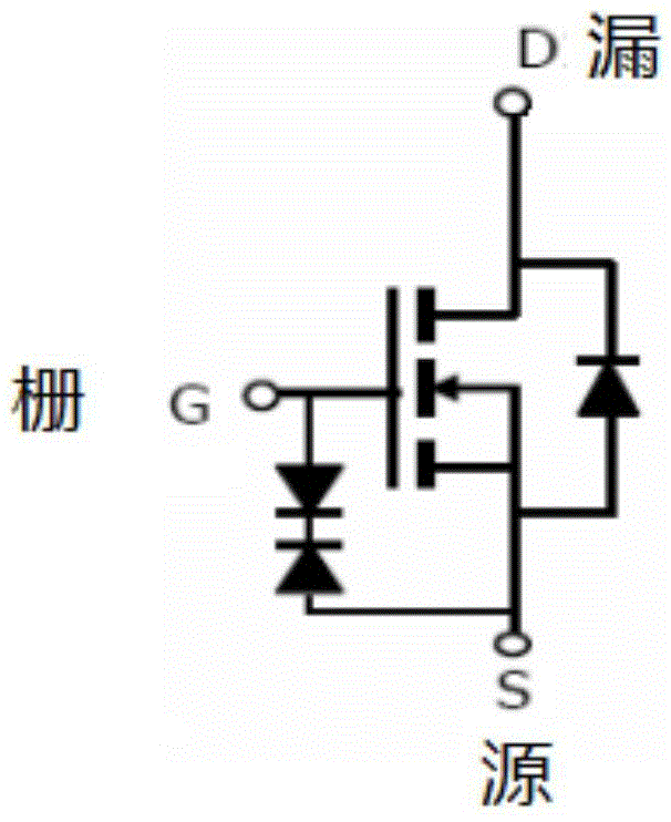
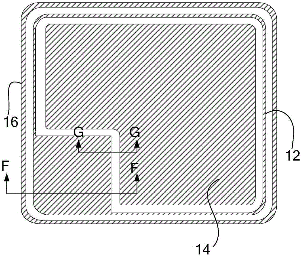
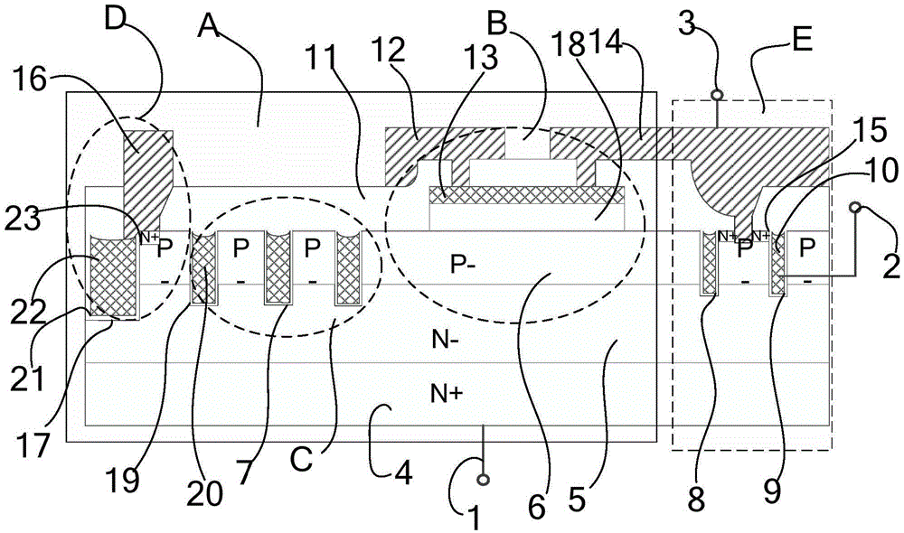
[0035] Such as figure 1 , figure 2 , image 3 and Figure 4 Shown: in order to improve the withstand voltage of devices with ESD protection and reduce manufacturing costs, taking an N-type low-voltage MOSFET device as an example, the present invention includes a cell region E and a terminal on the semiconductor substrate on the top view plane of the MOSFET device In the protected area A, the cellular area E is located in the central area of ​​the semiconductor substrate, and the terminal protected area A is located in the outer circle of the cellular area and surrounds the cellular area A; the terminal protected area A includes the adjacent cellular area A An electrostatic protection zone B; on the cross section of the MOSFET device, the semiconductor substrate includes an upper N-type drift region 5 and a lower N+ substrate 4, the N+ substrate 4 is adjacen...


PUM


Abstract

The invention relates to a low-voltage MOSFET device with an antistatic protection structure and a manufacturing method therefor. A static protection region comprises a second conductive type well region positioned at the upper part of a first conductive type drift region, and an insulating supporting layer positioned above the second conductive type well region; the second conductive type well region penetrates through a terminal protection region; the insulating supporting layer is positioned on a first main surface of a semiconductor substrate and is in contact with the second conductive type well region; a polycrystalline silicon diode group is arranged on the insulating supporting layer; the polycrystalline silicon diode group comprises a first diode and a second diode; the negative electrode end of the first diode is connected with the negative electrode end of the second diode; the positive electrode end of the first diode is in ohmic contact with the a grid electrode metal on the upward side; and the positive electrode end of the second diode is in ohmic contact with the a source electrode metal on the upward side. The low-voltage MOSFET device is compact in structure, compatible with the existing technological steps, safe, reliable, and capable of improving the voltage resistance of the device with ESD (Electro-static Discharge) protection and reducing manufacturing cost.

Description

technical field [0001] The invention relates to a MOSFET device and a manufacturing method thereof, in particular to a low-voltage MOSFET device with an antistatic protection structure and a manufacturing method thereof, belonging to the technical field of semiconductor MOSFET devices. Background technique [0002] Power MOSFET devices are prone to electrostatic discharge (Electro-Static discharge) during packaging, packaging, transportation, assembly and use. Static electricity will cause the breakdown of the insulating medium between the gate and the source, resulting in device failure. In pursuit of higher yield and device reliability, more and more MOSFETs require ESD protection design. [0003] The general design method in the existing process design is to connect a polysilicon diode group in parallel between the gate and the source. When static electricity occurs, the diode group can be broken down before the gate oxide layer and instantly discharge the voltage and cur...

Claims


Application Information

Patent Timeline
Patent Type & Authority Applications(China)
IPC IPC(8): H01L29/78H01L29/06H01L21/336
CPCH01L29/7811H01L29/0619H01L29/66712H01L29/7804H01L29/7808
Inventor 朱袁正周永珍
Owner WUXI NCE POWER
Why Eureka
Try Eureka