Preparation for SiGe HBT transistor

A transistor and polysilicon layer technology, applied in semiconductor/solid-state device manufacturing, electrical components, circuits, etc., can solve problems such as the deterioration of the cut-off frequency of the device performance, and achieve the effect of reducing the composite current of the base region, optimizing the effect, and achieving a good effect.

Active Publication Date: 2009-06-17
SHANGHAI HUAHONG GRACE SEMICON MFG CORP
View PDF0 Cites 16 Cited by
  • Summary
  • Abstract
  • Description
  • Claims
  • Application Information

AI Technical Summary

Problems solved by technology

The main challenge in optimizing the linearity of the device is not to significantly deteriorate the other properties of the device, especially the cutoff frequency

Method used


Image

  • Preparation for SiGe HBT transistor
  • Preparation for SiGe HBT transistor
  • Preparation for SiGe HBT transistor

Examples


Embodiment Construction

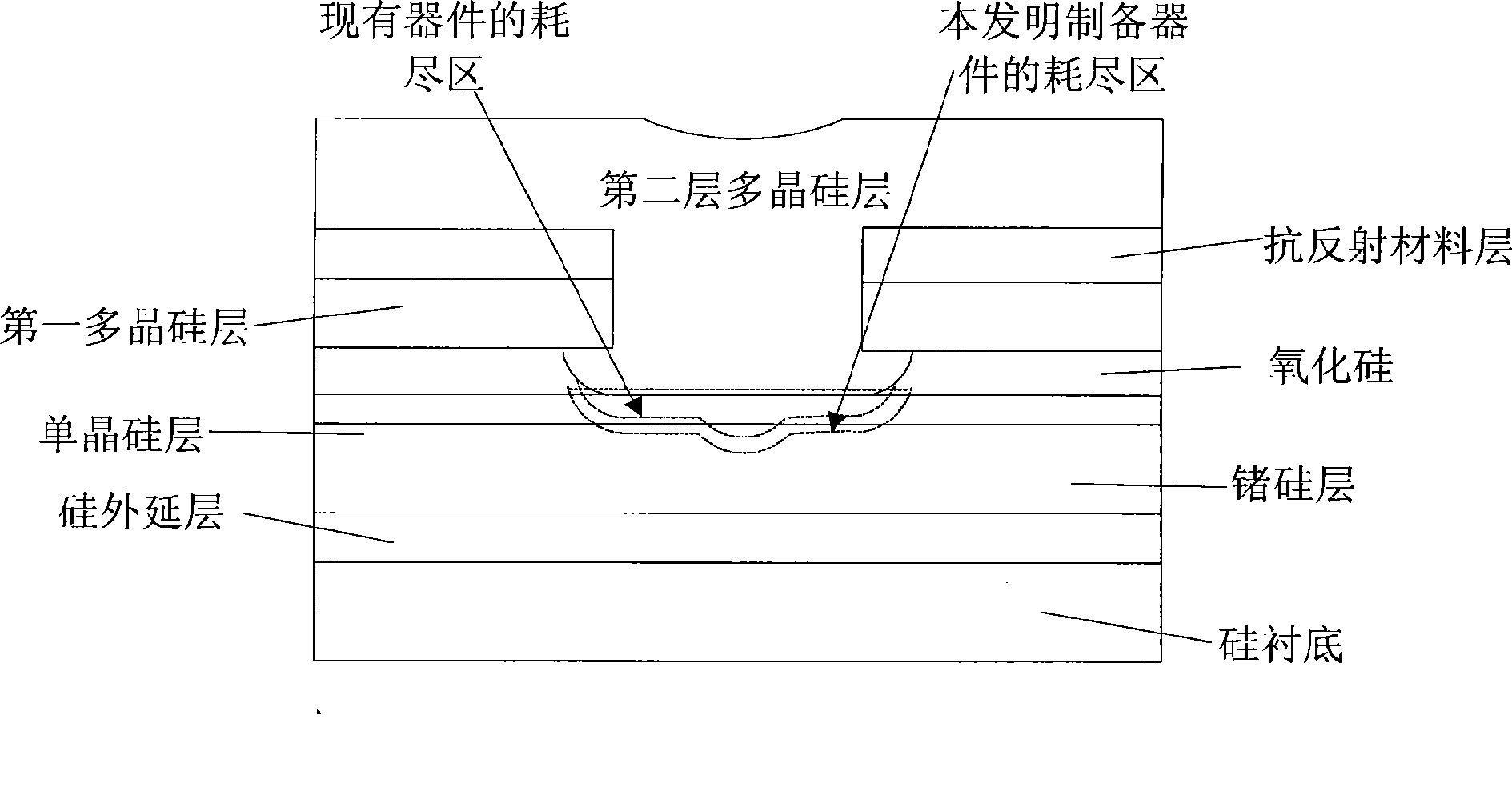
[0013] figure 1 It is a partial cross-sectional schematic diagram of the SiGe HBT transistor structure. The SiGe HBT transistor consists of an emitter polysilicon, an interface oxide layer between polysilicon and monocrystalline silicon, an emitter monocrystalline silicon (also called a capping layer), a silicon germanium base, and a collector. not shown). The silicon germanium base includes: the base layer of silicon (i.e., the silicon epitaxial layer), which is mainly used for the buffering of the silicon substrate to reduce defects; the silicon germanium core layer is used as the base area, wherein the silicon germanium core layer includes the germanium concentration rapid rise region, There are three parts, the platform area and the step-down area. The emitter single crystal silicon located on the contact surface between the base and the emitter is used for doping impurity arsenic ions in the polycrystalline silicon to diffuse to the single crystal silicon to form a singl...


PUM


Abstract

The invention discloses a method of producing SiGe HBT transistors, which includes steps of reducing the doping concentration of emitter polysilicon, controlling the undercut dimension of an emitter window, increasing the thickness of an emitter monocystal silicon layer, and increasing the final activation temperature of devices, thereby maintaining bases out of highly defective areas and further greatly reducing the base recombination current.

Description

technical field [0001] The invention relates to a preparation method of a SiGe HBT transistor, in particular to a preparation method for improving the linearity of the SiGe HBT transistor. Background technique [0002] Introducing Ge into the Si material to form a SiGe alloy semiconductor to adjust its energy band structure, as the base region of the bipolar transistor, this tube is called SiGe HBT (Silicon Germanium Heterojunction Bipolar Transistor). It is widely used in RF front-end components of communication systems. The main requirement for devices in RF applications is the highest possible cutoff frequency for a given breakdown voltage. The cutoff frequency is mainly determined by the base transit time and the collector RC delay. This device has the advantages of high linearity (low distortion), high cutoff frequency (speed), low noise, high power gain, and high spectral purity. Device linearity refers to the variation range of the collector current corresponding t...

Claims


Application Information

Patent Timeline
Patent Type & Authority Applications(China)
IPC IPC(8): H01L21/331
Inventor 陈帆周正良
Owner SHANGHAI HUAHONG GRACE SEMICON MFG CORP
Why Eureka
Try Eureka