Phosphorescent organic electroluminescent device

A luminescent and electromechanical technology, applied in the field of organic electroluminescent devices, can solve the problems of cost increase, device efficiency attenuation, high doping concentration of phosphorescent materials, etc., and achieve the goal of improving stability, maintaining long life and high efficiency, and reducing doping concentration Effect

Active Publication Date: 2017-06-27
KUNSHAN GO VISIONOX OPTO ELECTRONICS CO LTD +1
View PDF0 Cites 16 Cited by
  • Summary
  • Abstract
  • Description
  • Claims
  • Application Information

AI Technical Summary

Problems solved by technology

[0004] In the phosphorescent device where the traditional host is located, the excitons are transferred from the triplet state of the host to the triplet state of phosphorescence through the short-range Dexter, which leads to a high doping concentration of the phosphorescent material (10wt%~30wt%), high doping concentration It can reduce the distance between the host and the guest and promote the complete transfer of energy. However, too high a concentration will lead to attenuation of device efficiency. At the same time, the phosphorescent materials are all noble metal materials, and the higher doping concentration of phosphorescent dyes will increase the cost.

Method used


Image

  • Phosphorescent organic electroluminescent device
  • Phosphorescent organic electroluminescent device
  • Phosphorescent organic electroluminescent device

Examples


Embodiment 1

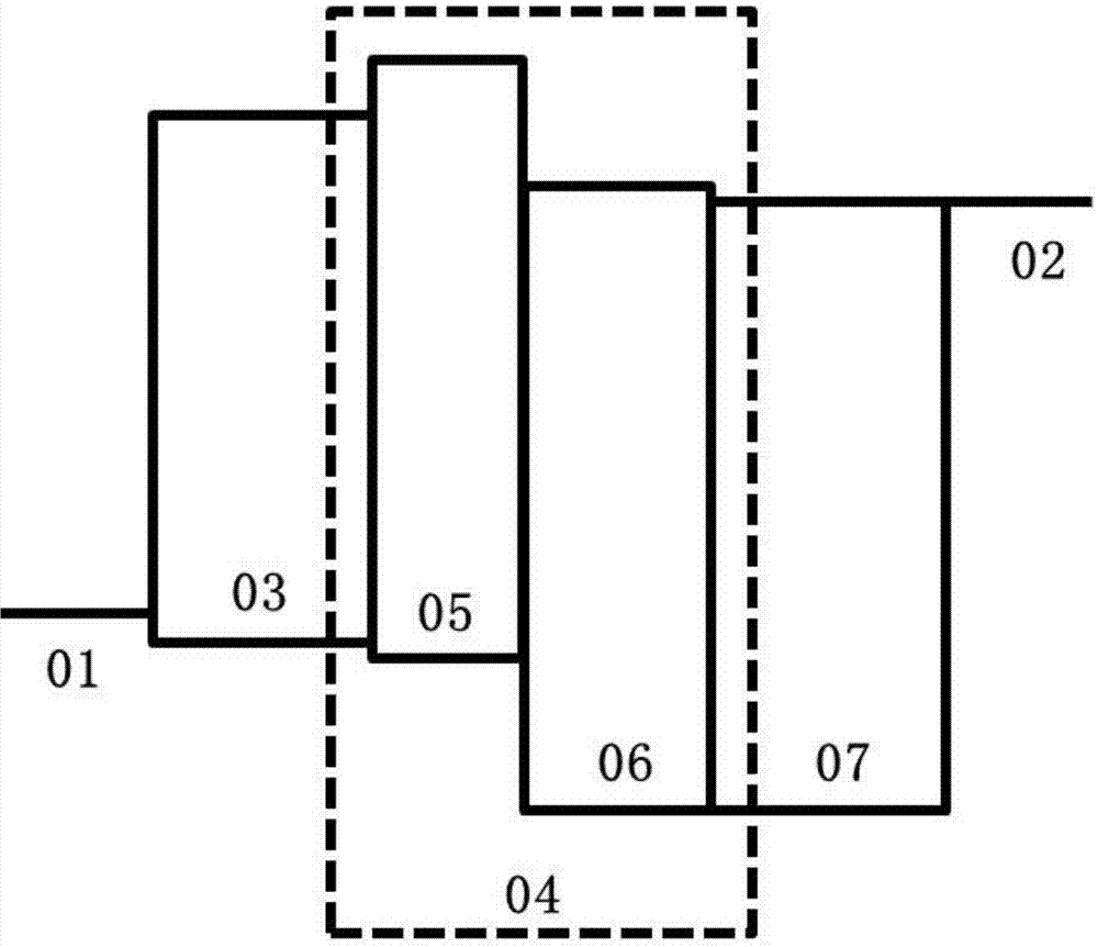
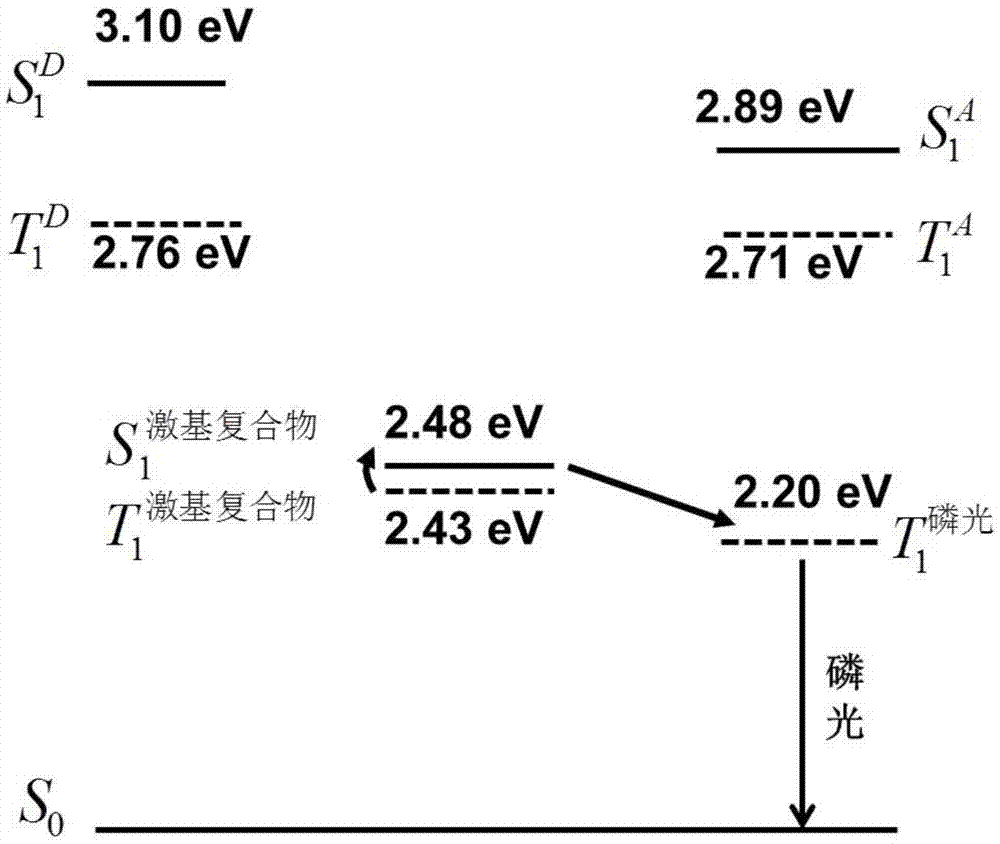
[0146] In this example, light-emitting devices with different thicknesses of the hole-transport material layer 05 and the electron-transport material layer 06 in the light-emitting layer were prepared. These devices have the following properties: figure 1 structure shown. Hole transport material layer 05 (composed of host material 2-5TCTA), electron transport material layer 06 (host material 1-8CzTrz, phosphorescent dye PO-01) of the light emitting layer. (The LUMO difference between the donor host and the acceptor host is greater than 0.3 eV, and the HOMO difference is greater than 0.2 eV; the first singlet energy level of the exciplex is higher than that of the phosphorescent dye.) Phosphorescent dye PO-01 The proportion in the light-emitting layer is 3wt%.

[0147] The device structure of this embodiment is as follows:

[0148] ITO (150nm) / NPB (40 nm) / hole transport material layer TCTA (10 nm) / electron transport material layer 1-8CzTrz+phosphorescent dye PO-01 (30nm) / Bphe...

Embodiment 2

[0169] The device structure of this embodiment is as follows:

[0170] ITO(150nm) / NPB(40nm) / TCTA(10nm) / CzTrz+1~10wt% phosphorescent dye PO-01(30nm) / Bphen(20nm) / LiF(0.5nm) / Al(150nm)

[0171] The proportion of phosphorescent dye PO-01 in the light-emitting layer is 1-10wt%.

[0172] In this embodiment, different doping concentrations of phosphorescent dyes are selected for experiments in the light-emitting layer, and the results shown in Table 2 are obtained.

[0173] Table 2

[0174] luminous layer Luminous efficiency (cd / A) Brightness (cd / m 2 )

[0175] It can be seen from Table 2 that when the doping concentration of the phosphorescent dye in the light-emitting layer is 3wt%, the external quantum efficiency and lifetime of the OLED device are both optimal.

Embodiment 3

[0177] In order to test the influence of the host material of the present invention on the performance of the organic electroluminescent device, this example prepared an organic electroluminescent device in the same manner as in Example 1 above. The structure of the light emitting device is as follows:

[0178] ITO (150nm) / NPB (40 nm) / hole transport material layer (material with hole transport ability) (10 nm) / electron transport material layer (material with electron transport ability: 3wt% phosphorescent dye) (30 nm ) / Bphen(20nm) / LiF(0.5nm) / Al(150nm)

[0179] The proportion of phosphorescent dye PO-01 in the light emitting layer is 3wt%.

[0180] The properties of the organic electroluminescent device are shown in Table 3 below:

[0181] table 3

[0182] device hole transport material layer electron transport material layer Luminous efficiency (cd / A) Brightness (cd / m 2 )

[0183] It can be seen from Table 3 that the exciplexes formed between the interfac...


PUM


Abstract

The invention discloses a phosphorescent organic electroluminescent device, and the device comprises a hole transmission layer, a light emitting layer and an electron transmission layer, wherein the hole transmission layer, the light emitting layer and the electron transmission layer are stacked sequentially. The light-emitting layer is of a double-layer structure which consists of a hole transmission material layer and an electron transmission material layer. The hole transmission material layer is disposed between the hole transmission layer and the electron transmission material layer, and the electron transmission material layer is disposed between the hole transmission material layer and the electron transmission layer. A contact interface of the hole transmission material layer and the electron transmission material layer forms a laser-based composite. The hole transmission material layer comprises a main material, and the main material is a material with the capability of hole transmission. The electron transmission material layer comprises a main material and phosphorescent dye doped in the main material, wherein the main material is a material with the capability of electron transmission. The phosphorescent doped density is reduced through the laser-based composite, and the long service life and high efficiency can be maintained.

Description

technical field [0001] The invention belongs to the field of organic electroluminescent devices, in particular to a phosphorescent organic electroluminescent device. Background technique [0002] Organic electroluminescent devices have attracted widespread attention due to their thin body, large area, full curing, and flexibility, and their great potential in solid-state lighting sources and liquid crystal backlights has become a research hotspot. [0003] As early as the 1950s, Bernanose.A et al. started research on organic electroluminescent devices (OLEDs). The material initially studied was an anthracene single crystal. Due to the problem of the large thickness of a single wafer, the required driving voltage is very high. Until 1987, Deng Qingyun (C.W.Tang) and Vanslyke of Eastman Kodak Company in the United States reported the structure as: ITO / Diamine / Alq 3 / Mg:Ag organic small molecule electroluminescence device, the brightness of the device can reach 1000 cd / m at ...

Claims


Application Information

Patent Timeline
Patent Type & Authority Applications(China)
IPC IPC(8): H01L51/50H01L51/52H01L51/54
CPCH10K85/00H10K50/00H10K50/11H10K2101/40H10K30/865H10K50/80H10K85/631H10K85/633H10K85/654H10K85/6565H10K85/6576H10K85/6572H10K50/165H10K2101/90C07D333/76C07D401/14C07D403/14C09K11/06H10K50/125H10K50/15H10K2101/27H10K2101/30H10K50/18H10K85/60H10K85/324H10K85/342H10K2101/10
Inventor 段炼张东东刘嵩赵菲
Owner KUNSHAN GO VISIONOX OPTO ELECTRONICS CO LTD
Why Eureka
Try Eureka