High voltage and low on-resistance LDMOS transistor having radiation structure and isolation effect

Inactive Publication Date: 2006-02-16
SEMICON COMPONENTS IND LLC
View PDF6 Cites 19 Cited by
  • Summary
  • Abstract
  • Description
  • Claims
  • Application Information

AI Technical Summary

Benefits of technology

[0006] A high voltage LDMOS transistor according to the present invention includes a P-substrate. A first diffusion region and a second diffusion region containing N conductivity-type ions form an N-well in the P-substrate. The first diffusion region further develops an extended drain region. A drain diffusion region containing N+ conductivity-type ions forms a drain region in the extended drain region. A third diffusion region containing P conductivity-type ions forms separated P-field blocks located in the extended drain region. The P-field blocks have different sizes. A smallest size P-field block is nearest to the drain region. A source diffusion region having N+ conductivity-type ions forms a source region in the N-well which is formed by the second diffusion region. A contact diffusion region containing P+ conductivity-type ions forms a contact region in the N-well which is formed by the second diffusion region. A fourth diffusion region containing P conductivity-type ions forms an isolation P-well in the N-well which is formed by the

Problems solved by technology

However, the drawback of these prior arts is that aforementioned LDMOS transistors have higher on-resistance.
Although a high voltage and low on-resistance LDMOS transistor can be manufactured, the complexity of the production processes increases the production cost and/or reduces

Method used


Image

  • High voltage and low on-resistance LDMOS transistor having radiation structure and isolation effect
  • High voltage and low on-resistance LDMOS transistor having radiation structure and isolation effect
  • High voltage and low on-resistance LDMOS transistor having radiation structure and isolation effect

Examples


first embodiment

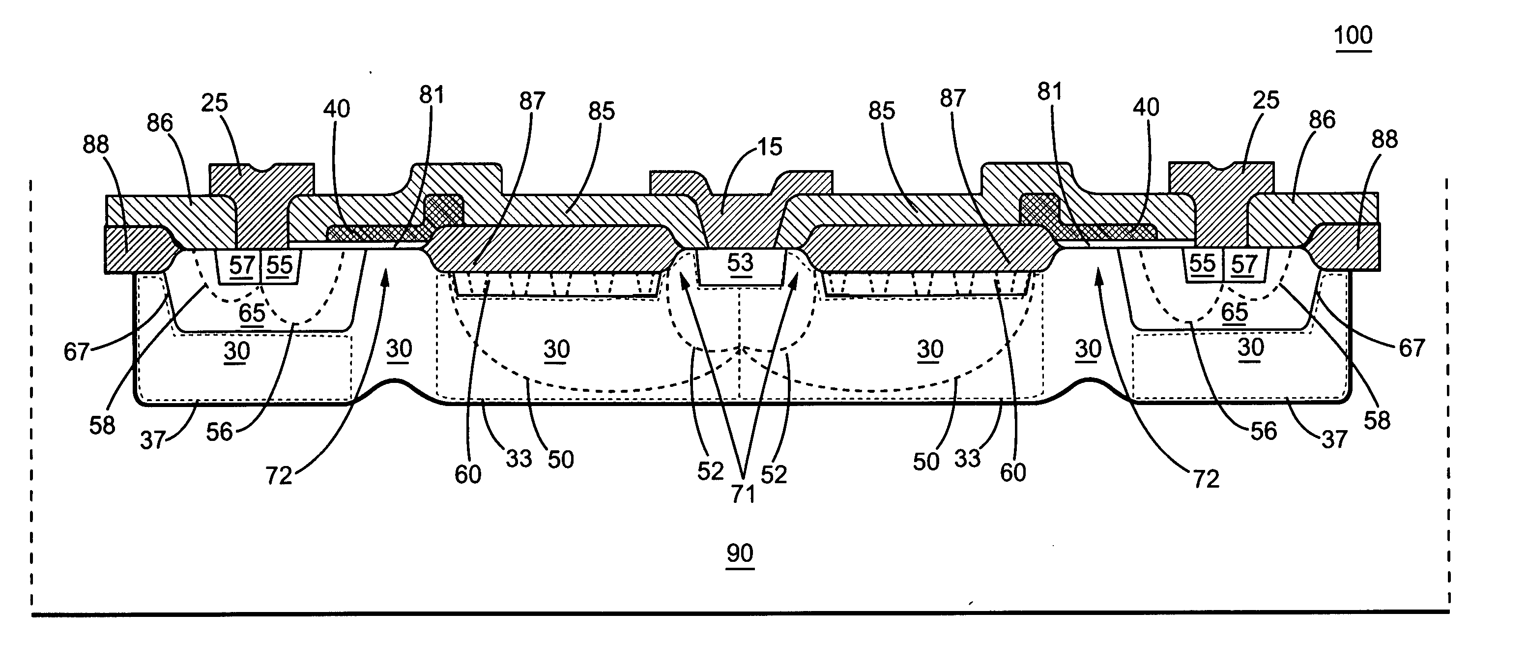
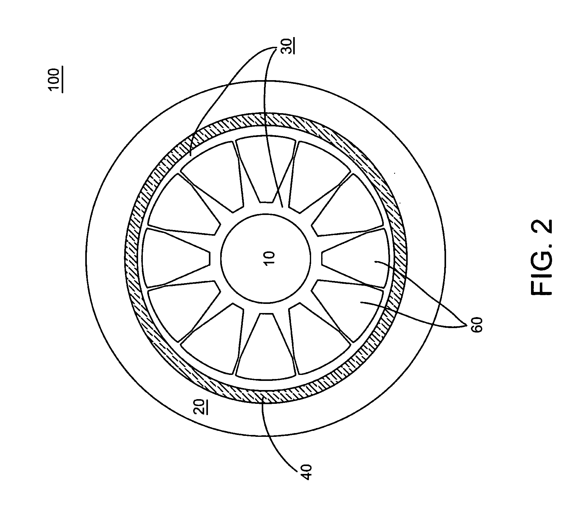
[0018]FIG. 2 shows the present invention, which is a top view of the LDMOS transistor 100. According to this embodiment, the LDMOS transistor 100 is in circular shape. The LDMOS transistor 100 includes a drain 10, a source 20 and a gate 40. Referring to FIG. 1 and FIG. 2, the extended drain region 50 and the drain diffusion region 53 both form the drain 10. The isolation P-well 65, the source diffusion region 55 and the contact diffusion region 57 form the source 20. The N-well 30 enclosing the P-field block 60 is connected from the drain 10 to the source 20. The portion of the N-well 30 located in between a plurality of P-field block 60 reduces the on-resistance of the channel.

[0019] The P-field block 60 is located in the extended drain region 50 of the N-well 30. The N-well 30, the P-field block 60 deplete the drift region, which build electrical fields in the N-well 30 to increase the breakdown voltage. In order to get higher breakdown voltage, the extended drain region 50 must b...

second embodiment

[0020]FIG. 3 shows the present invention, which is a top view of the LDMOS transistor 100. According to this embodiment, the LDMOS transistor 100 is in polygonal shape, e.g. a hexagon. Properly determining the length of side and interior angle of polygon facilitates the combination with other transistors as shown in FIG. 3. This could form a common source structure for die-space saving. A P-field block 602 located in the N-well 30 can be in suitable shape with suitable concentration for modulating to achieve high breakdown voltage and low on-resistance effects. The structure in FIG. 3 illustrates that the area use efficiency of wafer can be improved.

third embodiment

[0021]FIG. 4 shows the present invention, which is a top view of the LDMOS transistor 100. According to this embodiment, the LDMOS transistor 100 is in circular shape. The P-field blocks 604 and 606 located in a single radial direction within the N-well 30 are at least one block for modulating to achieve different breakdown voltage and on-resistance effects.


PUM


Abstract

A high voltage LDMOS transistor according to the present invention includes at least one P-field block in the extended drain region of the N-well. The P-field blocks form junction-fields in the N-well for equalizing the capacitance of parasitic capacitors between the drain region and the source region and fully deplete the drift region before breakdown occurs. A higher breakdown voltage is therefore achieved and the N-well having a higher doping density is thus allowed. The source region and P-field blocks enclose the drain region, which makes the LDMOS transistor self-isolated.

Description

BACKGROUND OF THE INVENTION [0001] 1. Field of the Invention [0002] The present invention relates to semiconductor devices, and more particularly to a lateral power MOSFET having radiation structure and isolation effect. [0003] 2. Description of Related Art [0004] The development of single chip process for integrating power switches with control circuitries is a major trend in the field of power IC development. The LDMOS (lateral double diffusion MOS) process in particular is currently being applied to manufacture monolithic ICs. The LDMOS process involves performing planar diffusion on the surface of a semiconductor substrate to form a main current path oriented in the lateral direction. [0005] In recent developments, many high-voltage LDMOS transistors have been proposed. However, the drawback of these prior arts is that aforementioned LDMOS transistors have higher on-resistance. Therefore, high voltage and low on-resistance LDMOS transistors are proposed. Although a high voltage ...

Claims


Application Information

Patent Timeline
IPC IPC(8): H01L29/76
CPCH01L29/0634H01L29/0692H01L29/7816H01L29/0886H01L29/42368H01L29/0696
Inventor HUANG, CHIH-FENGYANG, TA-YUNGLIN, JENN-YU G.CHIEN, TUO-HSIN
Owner SEMICON COMPONENTS IND LLC
Why Eureka
Try Eureka