

Semiconductor device provided with vertical semiconductor element
A semiconductor and device technology, applied in the field of semiconductor devices including vertical semiconductor elements
- Summary
- Abstract
- Description
- Claims
- Application Information
AI Technical Summary
Problems solved by technology
Method used
Image

Examples
no. 1 example )
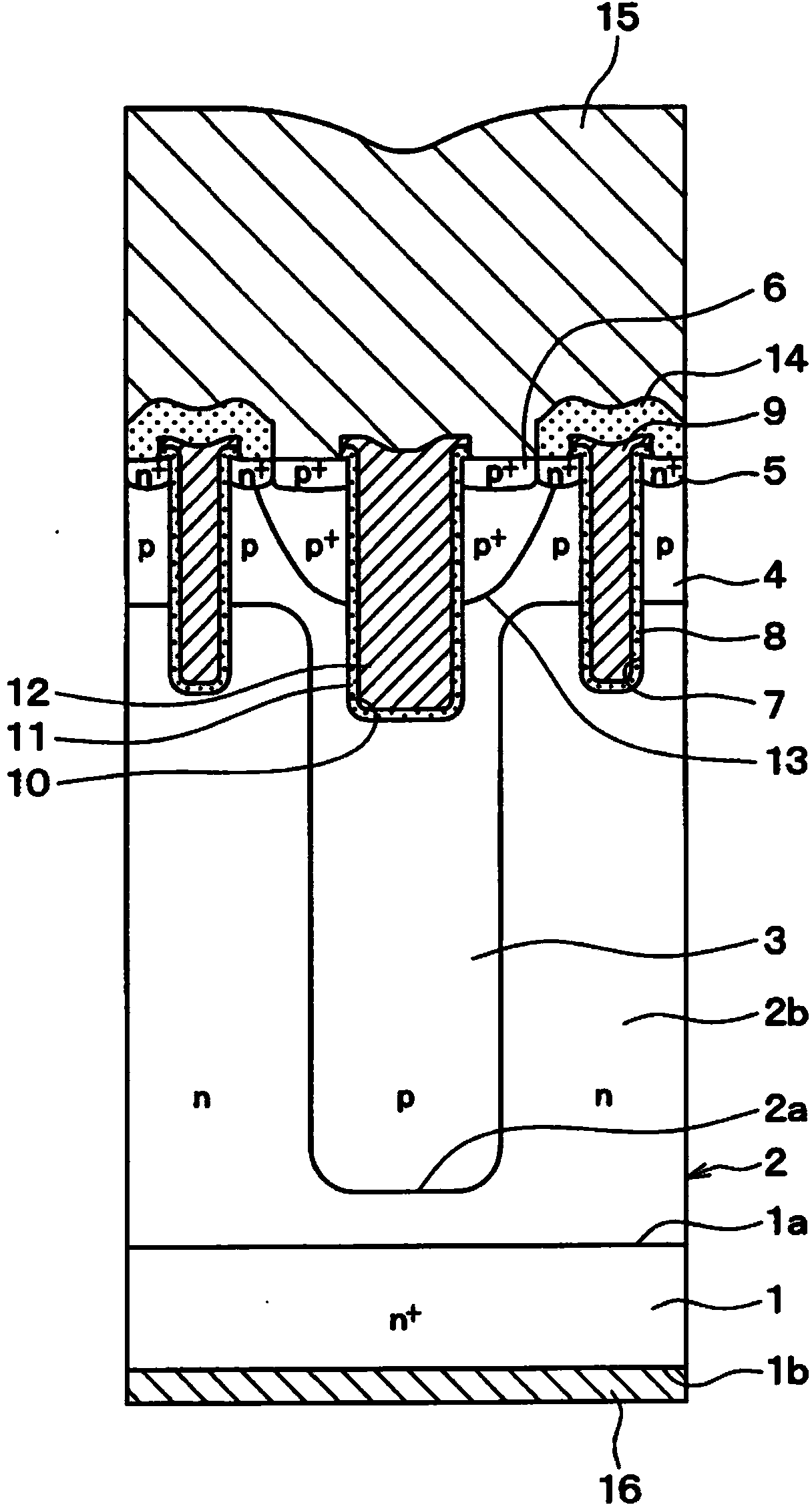
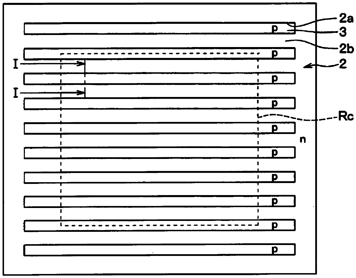
[0033] A first embodiment of the present disclosure will be described. In this embodiment, a semiconductor device including a vertical MOS transistor as a vertical semiconductor element will be described as an example. figure 1 is a cross-sectional view showing the cell region Rc of the semiconductor device including the vertical MOS transistor according to the present embodiment. figure 2 is showing figure 1 A diagram of the layout of the semiconductor device is shown. figure 1 corresponds to along figure 2 A cross-sectional view taken along line I-I in .
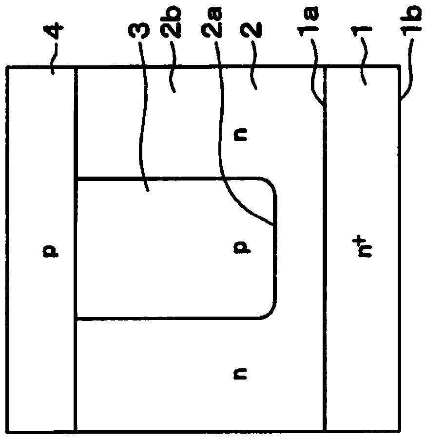
[0034] in accordance with figure 1 In the semiconductor device of the present embodiment shown, an inverted vertical MOS transistor having a trench gate structure is provided as the vertical MOS transistor. like figure 1 shown, using n + Type substrate 1 forms a vertical MOS transistor. in n + In the substrate 1, one surface is referred to as a main surface 1a, and the opposite surface is referred to as a rear s...
no. 2 example )
[0055] A second embodiment of the present disclosure will be described. In this embodiment, the configuration of the super junction structure is changed from that of the first embodiment, while other parts are similar to the first embodiment. Therefore, only parts different from the first embodiment will be described.
[0056] Figure 6 is a cross-sectional view showing the cell region Rc of the semiconductor device including the vertical MOS transistor according to the present embodiment. Such as Figure 6 As shown, in this embodiment, a dummy gate structure is formed at the position where the n-type region 2b is formed. Specifically, the longitudinal directions of the first trench 7 and the second trench 10 are set to be the same direction as the longitudinal directions of the n-type region 2 b and the p-type region 3 . First trench 7 is arranged in every other n-type region 2b, and second trench 10 is formed at a portion of n-type region 2b where first trench 7 is not f...
no. 3 example )
[0059] A third embodiment of the present disclosure will be described. In this embodiment, the configuration of the super junction structure is changed from that of the first embodiment, while other parts are similar to the first embodiment. Therefore, only parts different from the first embodiment will be described.
[0060] 7( a ) to 7( b ) are cross-sectional views showing the cell region Rc of the semiconductor device including the vertical MOS transistor according to the present embodiment. Figure 8 is a diagram showing the layout of the semiconductor device shown in FIG. 7 . Figure 7(a) and Figure 7(b) respectively correspond to the Figure 8 A cross-sectional view taken along lines VIIA-VIIA, VIIB-VIIB in .
[0061] Figure 7 (a), (b) and Figure 8 As shown, in this embodiment, the longitudinal direction of the first trench 7 and the second trench 10 is set to intersect the longitudinal direction of the n-type region 2b and the p-type region 3, so that the trench ga...
PUM
 Abstract
Description
Claims
Application Information