Capacitance dielectric layer, capacitor and forming method thereof

a technology of capacitor and dielectric layer, which is applied in the direction of capacitor, semiconductor device details, semiconductor/solid-state device, etc., can solve the problems of insufficient per-unit capacitance, data loss, and significant number of defects, so as to increase the capacitance per-unit area, reduce the breakdown voltage, and increase the leakage current

Active Publication Date: 2007-08-23
MARLIN SEMICON LTD
View PDF5 Cites 25 Cited by
  • Summary
  • Abstract
  • Description
  • Claims
  • Application Information

AI Technical Summary

Benefits of technology

[0008] Accordingly, at least one objective of the present invention is to provide a capacitance dielectric layer capable of preventing the problems of having an increase in the leakage current and a decrease in the breakdown voltage when the thickness of the capacitance dielectric layer is reduced to increase the capacitance per unit area.

Problems solved by technology

It should be noted that with the continuous reduction in device dimension, the capacitor structure inside some mixed mode devices or radio frequency (RF) devices may encounter the problem of not having enough per unit capacitance.
If the thickness of the capacitance dielectric layer is directly reduced using the same process, significant number of defects 130 such as seams or pinholes can easily form in the capacitance dielectric layer, particularly, the silicon nitride portion.
Ultimately, data may be lost and the processing reliability and yield may be affected.

Method used


Image

  • Capacitance dielectric layer, capacitor and forming method thereof
  • Capacitance dielectric layer, capacitor and forming method thereof
  • Capacitance dielectric layer, capacitor and forming method thereof

Examples


Embodiment Construction

[0040] Reference will now be made in detail to the present preferred embodiments of the invention, examples of which are illustrated in the accompanying drawings. Wherever possible, the same reference numbers are used in the drawings and the description to refer to the same or like parts.

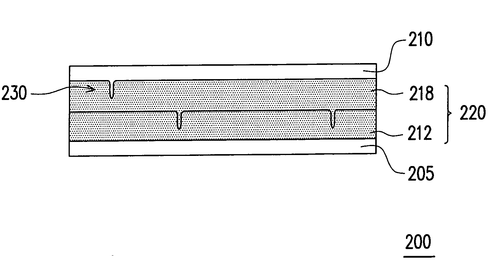
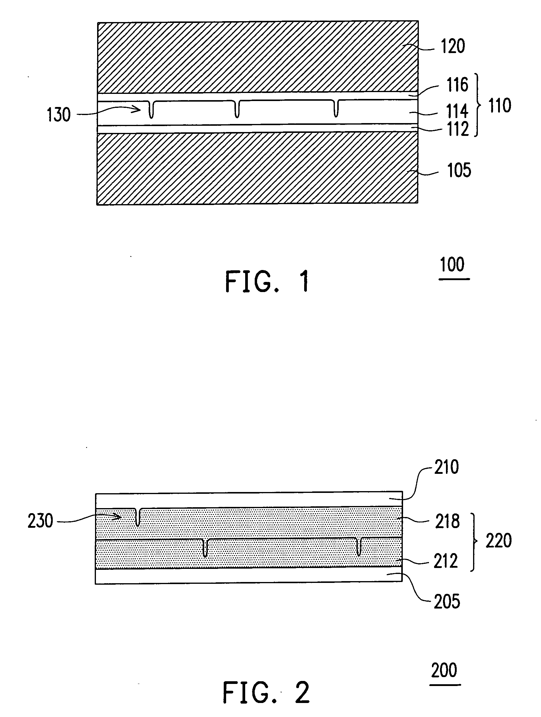
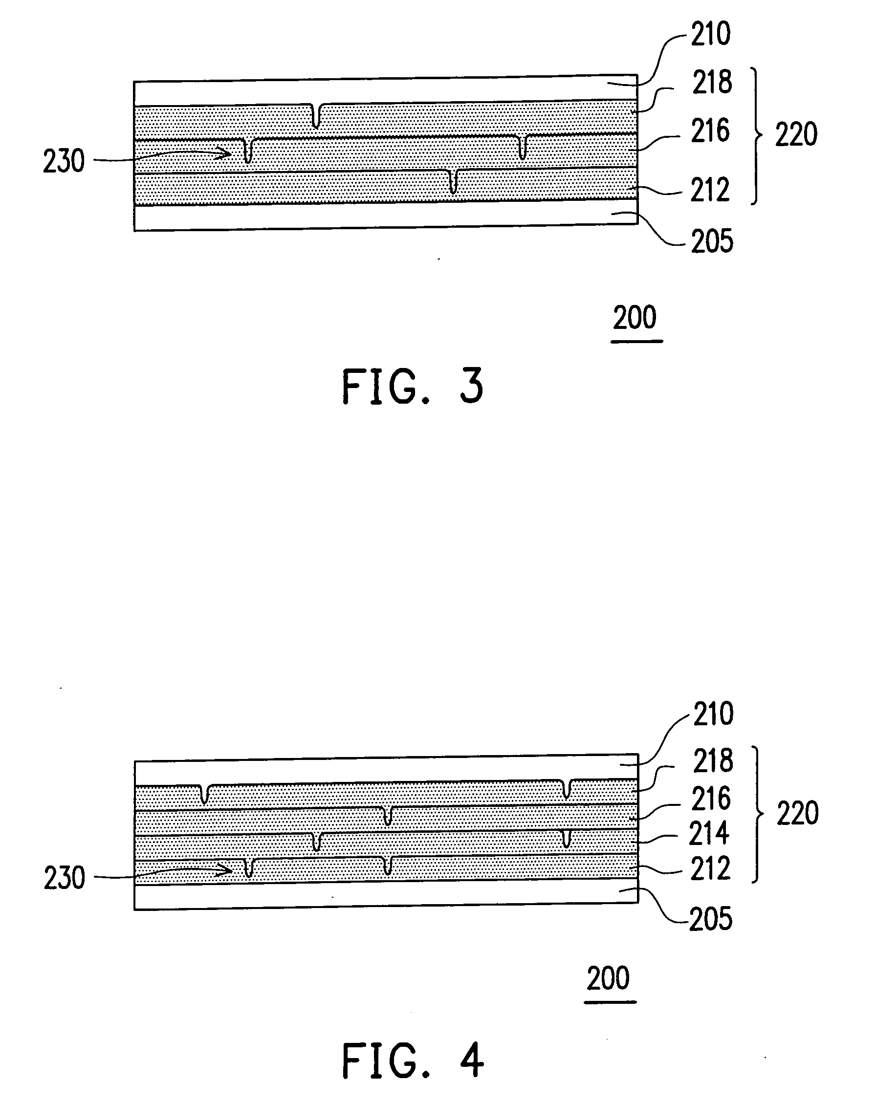
[0041]FIG. 2 is schematic cross-sectional view of a capacitance dielectric layer according to one embodiment of the present invention. The capacitance dielectric layer 200 as shown in FIG. 2 includes a first dielectric layer 205, a second dielectric layer 210 and a silicon nitride stacked layer 220. The first dielectric layer 205 can be fabricated using a material selected from a group consisting of silicon oxide, silicon nitride, silicon carbide, silicon oxynitride, silicon carbon nitride and silicon carbon oxide, for example. Similarly, the second dielectric layer 210 can be fabricated using a material selected from a group consisting of silicon oxide, silicon nitride, silicon carbide, silicon ox...


PUM

PropertyMeasurementUnit
capacitanceaaaaaaaaaa
dielectricaaaaaaaaaa
metallicaaaaaaaaaa

Abstract

A capacitance dielectric layer is provided. The capacitance dielectric layer includes a first dielectric layer, a second dielectric layer and a silicon nitride stacked layer. The silicon nitride stacked layer is disposed between the first dielectric layer and the second dielectric layer. The structure of the capacitance dielectric layer permits an increase in the capacitance per unit area by decreasing the thickness of the capacitance dielectric layer and eliminates the problems of having a raised leakage current and a diminished breakdown voltage.

Description

BACKGROUND OF THE INVENTION [0001] 1. Field of the Invention [0002] The present invention relates to a semiconductor device and forming method thereof. More particularly, the present invention relates to a capacitance dielectric layer, a forming method thereof and a capacitor. [0003] 2. Description of the Related Art [0004] In recent years, with the rapid development of integrated circuit manufacturing industry, the miniaturization of devices and the increase in the level of integration continue unabated. As a result, the design of circuit devices is advancing toward ever-decreasing dimensions. [0005]FIG. 1 is a schematic cross-sectional view of a conventional capacitor. In general, a capacitor 100 mainly comprises a bottom electrode plate 105, a capacitance dielectric layer 110 and a top electrode plate 120. The top electrode plate 120 and the bottom electrode plate 105 are mostly fabricated using polysilicon. The capacitance dielectric layer 110 is normally a three-layered structu...

Claims


Application Information

Patent Timeline
Patent Type & Authority Applications(United States)
IPC IPC(8): H01L21/8244
CPCH01L28/40H01L21/3185H01L21/02126H01L21/02167H01L21/02164H01L21/0214H01L21/022H01L21/02271H01L21/0217
Inventor WANG, CHIH-CHUNCHEN, HSIN-HSINGCHIANG, YU-HO
Owner MARLIN SEMICON LTD
Why Eureka
Try Eureka