An ldmos SCR device for integrated circuit chip esd protection

A technology for integrated circuits and devices, applied in the field of LDMOS SCR devices for ESD protection of integrated circuit chips, can solve problems such as device damage and voltage value reduction, and achieve the effects of process compatibility, enhanced ESD resistance, and improved latch-up immunity.

Inactive Publication Date: 2015-07-29
UNIV OF ELECTRONICS SCI & TECH OF CHINA
View PDF5 Cites 1 Cited by
  • Summary
  • Abstract
  • Description
  • Claims
  • Application Information

AI Technical Summary

Problems solved by technology

However, the maintenance voltage Vhold of this LDMOS SCR structure is greatly lower than the Vhold voltage value of ordinary LDMOS, which is far lower than the power supply voltage of the high-voltage power tube, which may easily cause a latch-up (latch_up) when the device is working normally, so that the device does not Controlled by the pre-driver, it may even lead to device damage

Method used


Image

  • An ldmos SCR device for integrated circuit chip esd protection
  • An ldmos SCR device for integrated circuit chip esd protection
  • An ldmos SCR device for integrated circuit chip esd protection

Examples


specific Embodiment approach 1

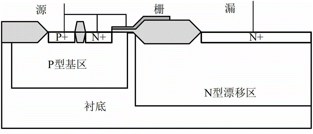
[0021] A kind of integrated circuit chip ESD protection LDMOS SCR device, such as image 3 As shown, it includes an nLDMOS device; the nLDMOS device includes an N-type drift region and a P-type base region located side by side on the substrate surface, wherein the N-type drift region and the P-type base region are in contact with each other or not; the P-type base region There is an N+ source region and a P+ contact region connected to the source metal in the region, wherein the N+ source region and the P+ contact region are in contact with each other or not; the side of the N-type drift region surface away from the P-type base region has a connection with the drain The metal-connected N+ drain region; the surface of the P-type base region between the N+ source region and the N-type drift region has a gate oxide layer, and the surface of the gate oxide layer has a polysilicon gate. The N-type drift region of the nLDMOS device also has a P well, and the existence of the P well ...

specific Embodiment approach 2

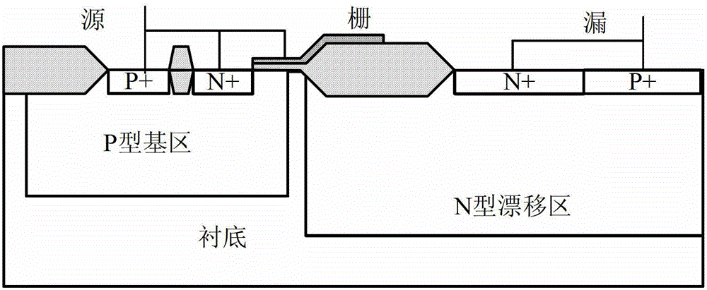
[0025] Such as Figure 5 shown, with image 3 Shown differently: simply put the figure 2 All the N-types in it are changed into P-type, and the P-type is changed into N-type, that is, the pLDMOS SCR device for ESD protection of integrated circuit chip provided by the present invention is obtained. The specific technical scheme is as follows:

[0026] A kind of integrated circuit chip ESD protection LDMOS SCR device, such as Figure 5 As shown, it includes a pLDMOS device; the pLDMOS device includes a P-type drift region and an N-type base region located side by side on the substrate surface, wherein the P-type drift region and the N-type base region are in contact with each other or not; the N-type base region There is a P+ source region and an N+ contact region connected to the source metal in the region, wherein the P+ source region and the N+ contact region are in contact with each other or not; the side of the P-type drift region surface away from the N-type base regio...


PUM


Abstract

The invention discloses an LDMOS SCR for protection against integrated circuit chip ESD protection and belongs to the technical field of electrons. According to the LDMOS SCR for the protection against the integrated circuit chip ESD, a low-voltage MOS is integrated on the basis of a traditional structure of the LDMOS SCR for the protection against the integrated circuit chip ESD and the low-voltage MOS is used for limiting a hole current injected from the positive electrode of the nested SCR, so that value of the holding voltage Vhold is improved and latch-up immune ability of the LDMOS SCR in high-voltage application is improved. In addition, compared with an ordinary LDMOS, the LDMOS SCR for the protection against the integrated circuit chip ESD is stronger in ability of the protection against the ESD due to the integrated SCR. Besides, the LDMOS SCR for the protection against the integrated circuit chip ESD and the Bipolar CMOS DMOS technology are compatible.

Description

technical field [0001] The invention belongs to the field of electronic technology, and relates to the design technology of an electrostatic discharge (ESD for short) protection circuit of a semiconductor integrated circuit chip, especially an embedded SCR (Silicon Controlled Rectifier, silicon controlled rectifier) ​​for ESD protection. SCR for short) LDMOS structure. Background technique [0002] In the field of intelligent power integrated circuits, LDMOS (Lateral Double-diffused MOS transistor) power transistors are widely used in output driver stages. figure 1 It is a traditional LDMOS structure diagram. Although the device size of LDMOS is large, it is easily damaged by ESD. This is due to the uneven turn-on of the parasitic BJT of the multi-finger structure of the LDMOS power transistor and the current collector effect, which makes its ESD performance not high, so it is necessary to add an additional ESD protection circuit. [0003] Such as figure 2 As shown, in ...

Claims


Application Information

Patent Timeline
Patent Type & Authority Patents(China)
IPC IPC(8): H01L23/60H01L27/07H01L29/78
Inventor 张波樊航曲黎明盛玉荣蒋苓利
Owner UNIV OF ELECTRONICS SCI & TECH OF CHINA
Why Eureka
Try Eureka