
Silicon-on-insulator (SOI) circuit ESD global protecting structure

An ESD protection, silicon-on-insulator technology, applied in circuits, circuit devices, emergency protection circuit devices, etc., can solve the problems of difficult circuit immunity, easy damage, poor ESD resistance of SOIMOS tubes, etc., to overcome the limited ESD current capability , Promote the effect of collaborative work

Active Publication Date: 2010-09-08
SEMICON MFG INT (SHANGHAI) CORP +1
View PDF0 Cites 1 Cited by
  • Summary
  • Abstract
  • Description
  • Claims
  • Application Information

AI Technical Summary

Problems solved by technology

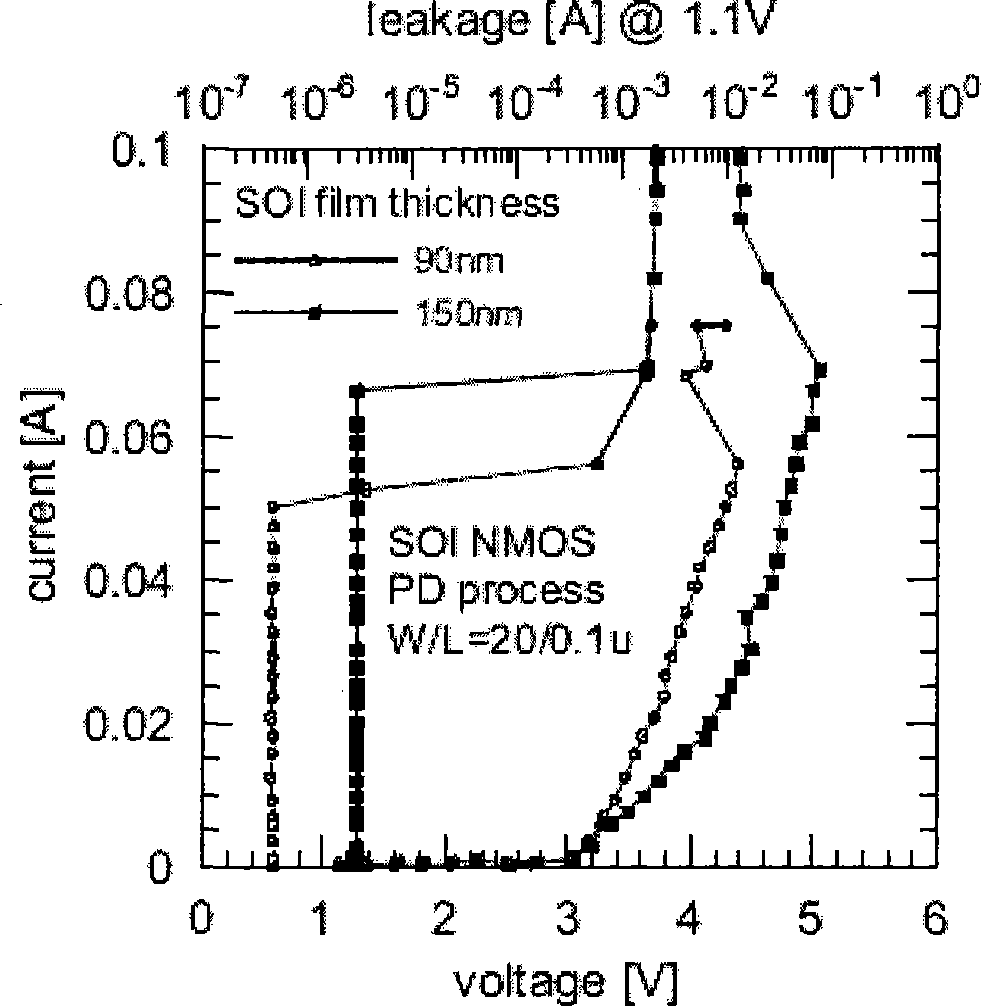
But in the SOI circuit, due to the very poor anti-ESD ability of the output tube, adding the effusion tube structure according to the method is like a drop in the bucket, and it is difficult to make the circuit reach 2000V ESD immunity.
[0005] In addition, due to the very poor ESD resistance of SOI MOS transistors, when the input terminal uses a MOS transistor with a smaller gate width as the secondary protection structure according to the bulk silicon technology, the secondary protection structure itself is also better than the secondary protection structure in the bulk silicon technology. more easily damaged

Method used


Image

  • Silicon-on-insulator (SOI) circuit ESD global protecting structure
  • Silicon-on-insulator (SOI) circuit ESD global protecting structure
  • Silicon-on-insulator (SOI) circuit ESD global protecting structure

Examples


Embodiment Construction

[0056] In order to make the object, technical solution and advantages of the present invention clearer, the present invention will be described in further detail below in conjunction with specific embodiments and with reference to the accompanying drawings.

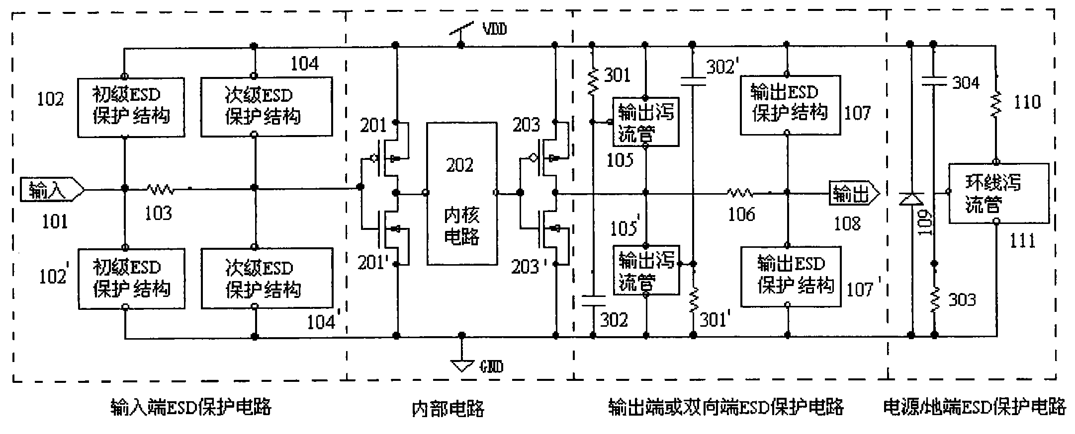
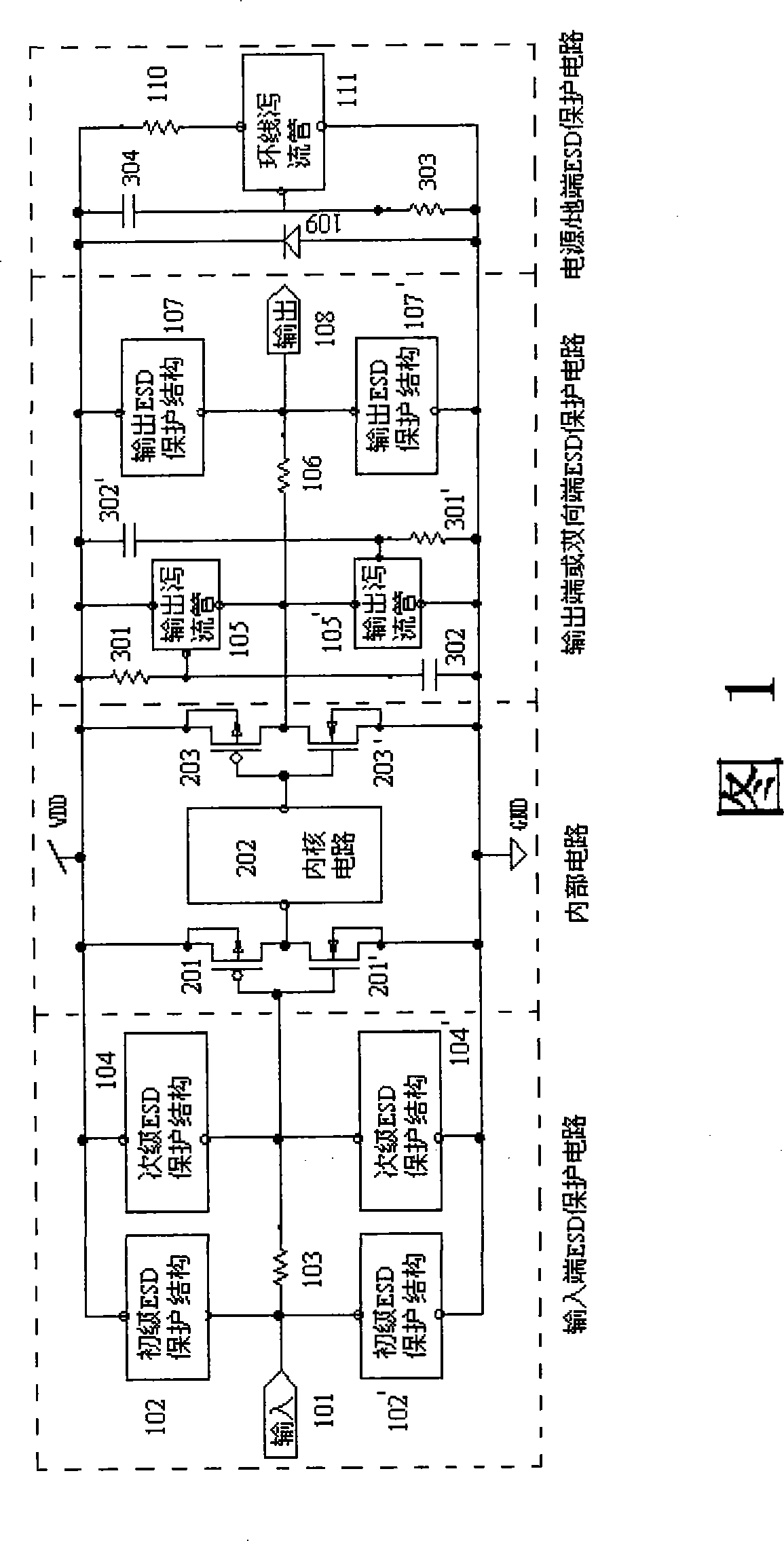
[0057] As shown in FIG. 1 , FIG. 1 is a schematic diagram of the overall ESD protection structure of the SOI circuit provided by the present invention. The ESD global protection structure includes two primary ESD protection structures 102 / 102' placed at the input end, two secondary ESD protection structures 104 / 104' placed at the input end, a primary ESD protection structure and a secondary ESD protection structure placed at the input end A resistance protection structure 103 between the protection structures, two output ESD protection structures 107 / 107' placed at the output end or bidirectional end, a drain electrode and output ESD protection of an output MOS transistor 203 / 203' placed at the output end or bidirectional ...


PUM


Abstract

The invention relates to the technical field of semiconductors and discloses a silicon-on-insulator (SOI) circuit ESD global protecting structure comprising the steps: a primary ESD protecting structure and a secondary ESD protecting structure protect an input end; an intelligent resistance ESD protecting structure, an output effusion pipe structure controlled by an RC circuit, and an output ESD protecting structure protect an output end / bi-directional end; a loop effusion pipe protecting structure controlled by the RC circuit and a serial intelligent resistance structure are arranged betweena power supply loop and an earth loop, used for protecting the power supply end and the earth end together with a parallel diode structure and assist the input end and the output end / bi-directional end to effuse ESD current. By using the invention, the problems that the SOI chip output end / bi-directional end has poor ESD current effusion capability and a single loop effusion pipe has limit capability for effusing the ESD current are solved so as to enable the ESD protecting capability of an SOI integrated circuit to be completely improved.

Description

technical field [0001] The invention relates to the technical field of semiconductors, in particular to a global protection structure for a silicon-on-insulator (SOI) circuit electrostatic discharge protection (ESD). Background technique [0002] With the development of the semiconductor industry, especially after entering the deep submicron scale, on the one hand, the breakdown voltage of the oxide layer will be greatly reduced; on the other hand, due to the characteristics of thin silicon film and poor heat dissipation of SOI technology, the leakage Terminal electrostatic discharge (ESD) protection capabilities have also become very poor. As a result, the ESD protection problem of the SOI circuit becomes very serious. [0003] In order to overcome this problem, the industry adopts SAB technical protection processing on the structure connected with the PAD. However, experiments have shown that although this method can effectively improve the ESD resistance of the circuit ...

Claims


Application Information

Patent Timeline
Patent Type & Authority Patents(China)
IPC IPC(8): H01L27/12H01L23/60H02H9/00
Inventor 曾传滨海潮和李晶李多力韩郑生
Owner SEMICON MFG INT (SHANGHAI) CORP
Learn More