Single-photon avalanche diode pixel structure and pixel array substrate

A single photon avalanche and pixel structure technology, applied in the electrical field, can solve the problems that it is difficult to evaluate the influence of the dark count rate of a single pixel structure, the single photon avalanche diode cannot detect the photon signal, and the avalanche effect occurs when excited, so as to facilitate crosstalk effect of influence

Active Publication Date: 2016-12-07
SHANGHAI ADVANCED RES INST CHINESE ACADEMY OF SCI
View PDF4 Cites 11 Cited by
  • Summary
  • Abstract
  • Description
  • Claims
  • Application Information

AI Technical Summary

Problems solved by technology

[0005] In view of the above-mentioned shortcomings of the prior art, the object of the present invention is to provide a single photon avalanche diode pixel structure and a pixel array structure, which are used to solve the problem of each single photon avalanche diode cathode in the prior art single photon avalanche diode array. The voltages are all above the critical avalanche voltage value, and the pixel structures that are not affected by the row selection control signal will still be stimulated to produce an avalanche effect, which will affect the normal operation of adjacent single photon avalanche diodes, so that the single photon avalanche diodes cannot be measured correctly. The problem of the photon signal, and because the exposure of the entire row is realized under the control of the row selection control signal, when measuring the dark count rate, it is difficult to evaluate the dark count rate of a single pixel structure and the impact on adjacent pixel structures after an avalanche of a single pixel structure The question of the impact

Method used


Image

  • Single-photon avalanche diode pixel structure and pixel array substrate
  • Single-photon avalanche diode pixel structure and pixel array substrate
  • Single-photon avalanche diode pixel structure and pixel array substrate

Examples


Embodiment 1

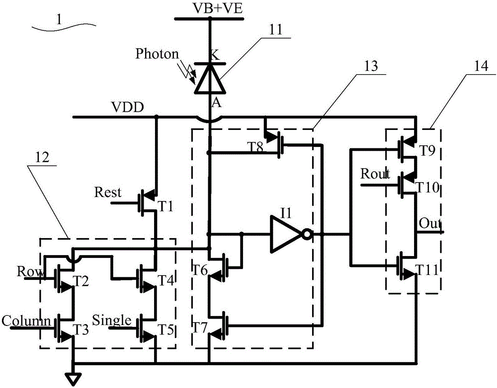
[0042] see figure 2 , the present invention provides a single photon avalanche diode pixel structure 1, the single photon avalanche diode pixel structure 1 includes: a single photon avalanche diode 11, the single photon avalanche diode 11 includes an anode and a cathode, figure 2 The anode of the single photon avalanche diode 11 is represented by A, and the cathode of the single photon avalanche diode 11 is represented by K; the cathode of the single photon avalanche diode 11 is connected with a bias voltage source (not shown), The bias voltage of the bias voltage source is VB+VE, wherein, VB is the critical avalanche voltage of the single photon avalanche diode 11, and VE is less than the power supply voltage VDD of the power supply; the first pull-up transistor T1, the second A pull-up tube T1 and a power supply (the power supply is not shown, figure 2 The power supply voltage VDD of the power supply is used as an illustration), the reset signal Rest and the anode of the...

Embodiment 2

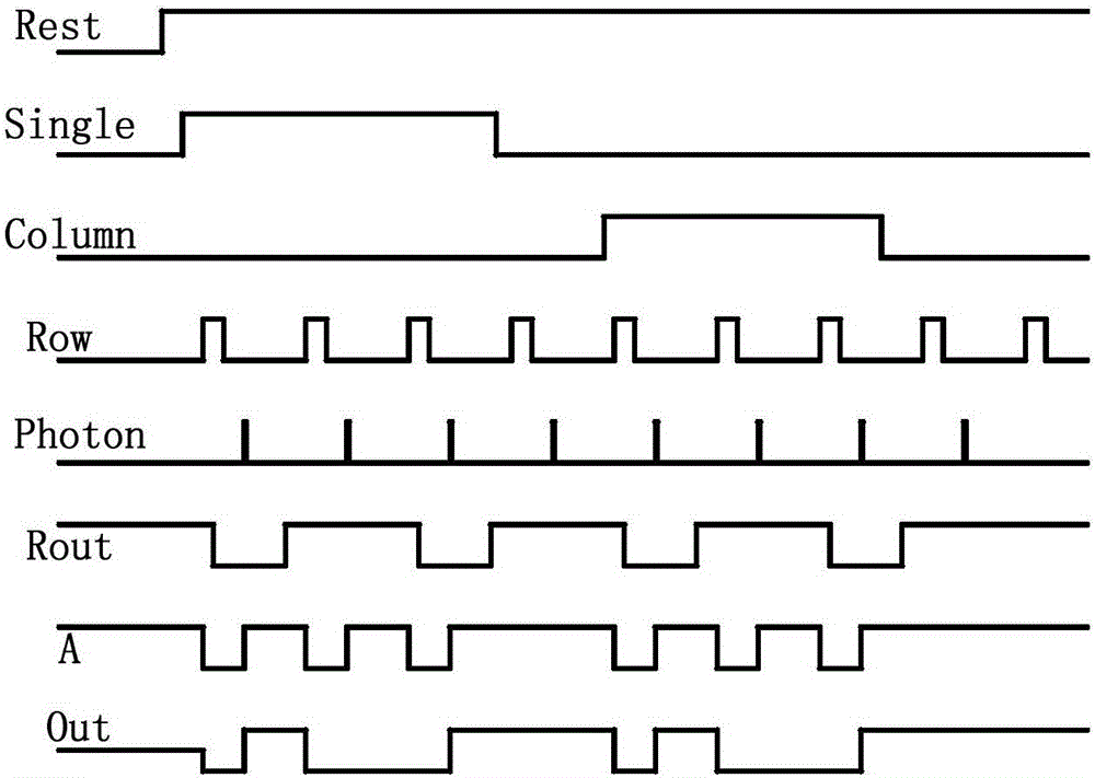
[0055] see Figure 4 , the present invention also provides a pixel array structure, the pixel array structure comprising: a plurality of single photon avalanche diode pixel structures 1 as described in any of the above schemes, and the single photon avalanche diode pixel structures 1 are distributed in an array; The single photon avalanche diode pixel structure 1 is connected to the row selection control signal Row, the column selection control signal Column, the row sharing signal Rout, the reset signal Rest and the single selection control signal Single; all the single photon avalanche diode pixel structures 1 The cathodes of the single photon avalanche diodes 11 are uniformly connected to a voltage whose voltage value is VE+VB, and all single photon avalanche diode pixel structures 1 share a power supply voltage VDD and a ground voltage GND.

[0056] As an example, Figure 4 It is taken as an example that the pixel array structure includes the single photon avalanche diode...


PUM


Abstract

The invention provides a single-photon avalanche diode pixel structure and a pixel array substrate. The single-photon avalanche diode pixel structure comprises a single-photon avalanche diode, a first pull-up tube, a pull-down tube unit, a quenching unit and an output unit, wherein the single-photon avalanche diode comprises an anode and a cathode; the cathode of the single-photon avalanche diode is connected with a bias voltage source; the first pull-up tube is connected with a power supply source, a reset signal and the anode of the single-photon avalanche diode; the pull-down tube unit is connected with the first pull-up tube and the anode of the single-photon avalanche diode; the quenching unit is connected with the power supply source, the pull-down unit and the anode of the single-photon avalanche diode; and the output unit is connected with the quenching unit. The single-photon avalanche diode pixel structure can bias voltage of the anode and the cathode of the single-photon avalanche diode below critical avalanche voltage when not selected for exposure and read-out, so that the avalanche effect is avoided. By the pixel array structure provided by the invention, exposure of a single pixel structure can be achieved; and research on the crosstalk effect of the single pixel structure on the adjacent pixel structure is facilitated.

Description

technical field [0001] The invention belongs to the field of electrical technology, and in particular relates to a single photon avalanche diode pixel structure and a pixel array structure. Background technique [0002] A single photon avalanche diode (SPAD) is a diode biased above a critical avalanche voltage, which can be used as a pixel unit of a 3D image sensor. The 3D image sensor based on SPAD can quickly acquire the 3D information of the object and realize 3D reconstruction. Dark count rate (DCR) is an important index to evaluate the performance of SPAD, especially the post-pulse and adjacent pixel crosstalk will greatly affect the working performance of SPAD array. [0003] Cristiano Niclass published a 3D CMOS image sensor based on SPAD pixel structure in JOURNAL OF SOLID-STATE CIRCUITS in 2008. The pixel structure of SPAD is as follows figure 1 shown. exist figure 1 Among them, the transistor M1 is controlled by the row selection control signal ROWSEL. When the...

Claims


Application Information

Patent Timeline
Patent Type & Authority Applications(China)
IPC IPC(8): H01L27/146
CPCH01L27/14643
Inventor 汪辉黄景林章琦汪宁田犁黄尊恺曹虎
Owner SHANGHAI ADVANCED RES INST CHINESE ACADEMY OF SCI
Why Eureka
Try Eureka