Light guide plate, backlight module and display device
A technology of backlight module and light guide plate, applied in the optical field, can solve the problems of light homogenization and brightness difference, and achieve the effect of improving light homogenization and brightness
- Summary
- Abstract
- Description
- Claims
- Application Information
AI Technical Summary
Problems solved by technology
Method used
Image
Examples
Embodiment 1
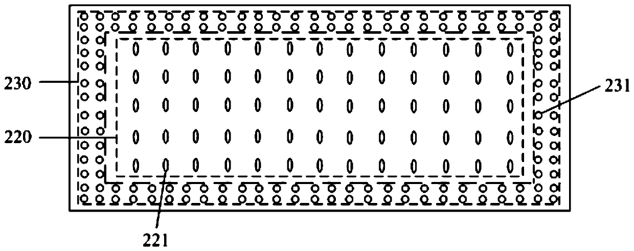
[0056] The light guide plate provided in this embodiment includes a substrate, a scattering part, and a light conversion part. The first surface of the substrate has grooves scattered and distributed, and the grooves form the scattering function structure of the scattering part. The light conversion part is arranged on the first surface, and the light conversion The light conversion functional structure of the part is arranged in the form of dispersed points, and the first surface is divided into a first sub-edge area, a second sub-edge area, a third sub-edge area, a fourth sub-edge area and a non-edge area, and the light conversion The scattering part is arranged in the four sub-edge regions, and the scattering part is arranged in the non-edge region.
[0057] Each sub-edge area has a row of equally spaced light-converting dots, the cross-sections of the light-converting dots and the scattering groove dots parallel to the first surface are circular, and the diameter ratio of t...
Embodiment 2
[0060] The light guide plate provided in this embodiment includes a substrate, a scattering part, and a light conversion part. The point form is set, the first surface is divided into the first sub-edge area, the second sub-edge area, the third sub-edge area, the fourth sub-edge area and the non-edge area, the light conversion part is arranged in the four sub-edge areas, and the scattering set in the non-marginal area.
[0061] Each sub-edge area is provided with a row of equally spaced light conversion network points, and the non-edge area is provided with equally spaced scattering network points. The diameter ratio of the scattering dots is 10:1. The materials forming the photoconverting functional structure are CdSe / ZnS core-shell quantum dots with an emission wavelength of 570nm and a silica gel matrix, wherein the concentration of the quantum dots is the same.
[0062] Wherein, the substrate is a PMMA substrate, and the material forming the scattering functional structu...
Embodiment 3
[0064]The difference between the light guide plate provided in this embodiment and Embodiment 2 is:
[0065] The light conversion part is arranged on the four sub-edge regions, and the scattering part is arranged on the non-edge region and the same four sub-edge regions as the light conversion part, and each sub-edge region has a row of scattering dots distributed at equal intervals, and is arranged on the edge region. The scattering dots and light conversion dots are arranged alternately.
PUM
| Property | Measurement | Unit |
|---|---|---|
| emission peak | aaaaa | aaaaa |
| refractive index | aaaaa | aaaaa |
| transmittivity | aaaaa | aaaaa |
Abstract
Description
Claims
Application Information


