
optical module

A technology of optical module and grating, applied in the field of optical communication

Active Publication Date: 2018-08-21
HISENSE BROADBAND MULTIMEDIA TECH
View PDF5 Cites 0 Cited by
  • Summary
  • Abstract
  • Description
  • Claims
  • Application Information

AI Technical Summary

Problems solved by technology

Therefore, it is impossible to control whether the DBR laser in SINK mode emits light through the laser transmitter driver chip in SINK mode

Method used


Image

  • optical module
  • optical module
  • optical module

Examples


Embodiment Construction

[0021] In order to make the purpose, technical solutions and advantages of the embodiments of the present invention clearer, the technical solutions in the embodiments of the present invention will be clearly and completely described below in conjunction with the drawings in the embodiments of the present invention. Obviously, the described embodiments It is a part of embodiments of the present invention, but not all embodiments. Based on the embodiments of the present invention, all other embodiments obtained by persons of ordinary skill in the art without creative efforts fall within the protection scope of the present invention.

[0022] Here, the application environment of the embodiment of the present invention is firstly introduced. The bias current of the laser transmitter driver chip involved in the embodiment of the present invention is the SINK mode, that is, the bias pin of the laser transmitter driver chip needs to have current poured in to drive whether the laser ...


PUM


Abstract

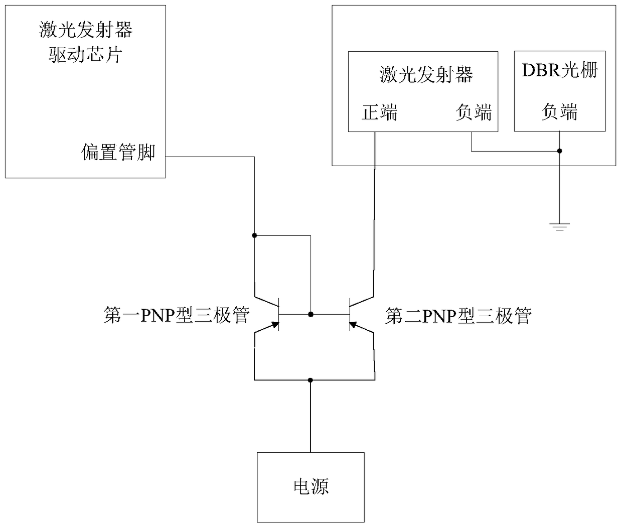
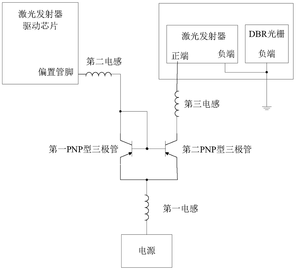
The invention provides an optical module. In this optical module, the emitters of the first PNP transistor and the second PNP transistor connected to the power supply are always at high level. When the bias pin of the laser transmitter driver chip is set at high level, the two PNP transistors The bases of the triodes are all at high level, in the cut-off state, no current flows into the bias pin and the laser emitter, and the laser emitter does not emit light; when the bias pin of the laser emitter drive chip is set to low level, both The bases of the two PNP transistors are all at low level and are in the conduction state, the current flows into the bias pin, and flows from the positive end of the laser emitter, and the laser emitter emits light. In the case that the laser transmitter driver chip and the laser transmitter are both in SINK mode, the power supply and two PNP transistors are used to simultaneously control whether the bias pin and the positive end of the laser transmitter have current inflow, thereby controlling the laser transmitter glowing.

Description

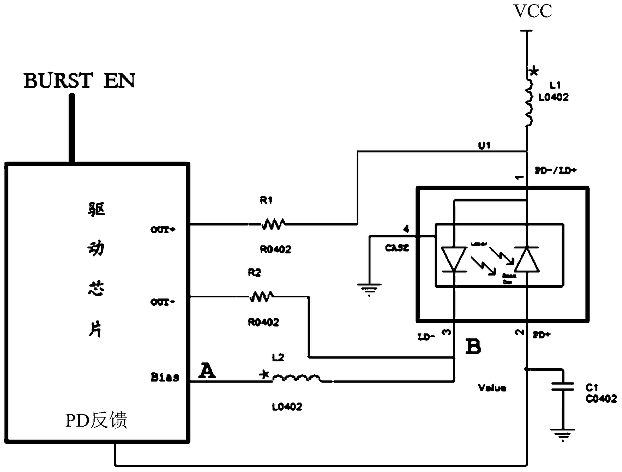
technical field [0001] The invention relates to the technical field of optical communication, in particular to an optical module. Background technique [0002] With the growth of people's demand for communication bandwidth, fiber-to-the-x (FTTx) technology has developed rapidly, and the fiber-to-the-x access technology based on passive optical network (Passive Optical Network, PON) technology has been widely used. [0003] A passive optical network usually includes an optical line terminal installed in a central control station, and optical network units (Optical Network Unit, ONU) installed in various user locations. The ONU is provided with a burst transmitting circuit for transmitting optical signals. figure 1 It is a schematic diagram of a burst transmitting circuit in the prior art. Such as figure 1 As shown, in the existing PON ONU, the burst emission circuit includes a driver chip and a distributed feedback laser (Distributed Feedback Laser, DFB), and the bias (Bia...

Claims


Application Information

Patent Timeline
Patent Type & Authority Patents(China)
IPC IPC(8): H04B10/50
CPCH01S5/0428H01S5/06256H01S5/068H01S5/06835H01S5/06832H01S5/125H01S5/0687H01S5/187H01S3/107H01S5/042
Inventor 闫洪平薛登山赵其圣李明
Owner HISENSE BROADBAND MULTIMEDIA TECH
Learn More