Method for detecting metal defect and method for forming detection structure

A metal defect and detection structure technology, which is applied in the manufacture of electrical components, circuits, semiconductors/solid-state devices, etc., can solve the problems of difficulty in addressing physical defects, time-consuming search for the physical location of metal defects, etc., and achieve high detection efficiency.

Active Publication Date: 2019-07-30
SEMICON MFG INT (SHANGHAI) CORP
View PDF3 Cites 0 Cited by
  • Summary
  • Abstract
  • Description
  • Claims
  • Application Information

AI Technical Summary

Problems solved by technology

[0002] With the continuous development of semiconductor integrated circuit device structure, the continuous improvement of process technology and the continuous reduction of device size, more and more defects in semiconductor integrated circuits are invisible. Using traditional defect detection methods to judge its failure mechanism and It is becoming more and more difficult to locate the physical defect address of the failure
[0003] For example, in the memory structure, the metal lines used as bit lines are usually larger than 100 microns, while the metal defects generated during the fabrication process are only 100 nanometers, which makes it time-consuming to find the physical location of the metal defects

Method used


Image

  • Method for detecting metal defect and method for forming detection structure
  • Method for detecting metal defect and method for forming detection structure
  • Method for detecting metal defect and method for forming detection structure

Examples


Embodiment Construction

[0030] In order to make the above objects, features and advantages of the present invention more comprehensible, specific embodiments of the present invention will be described in detail below in conjunction with the accompanying drawings.

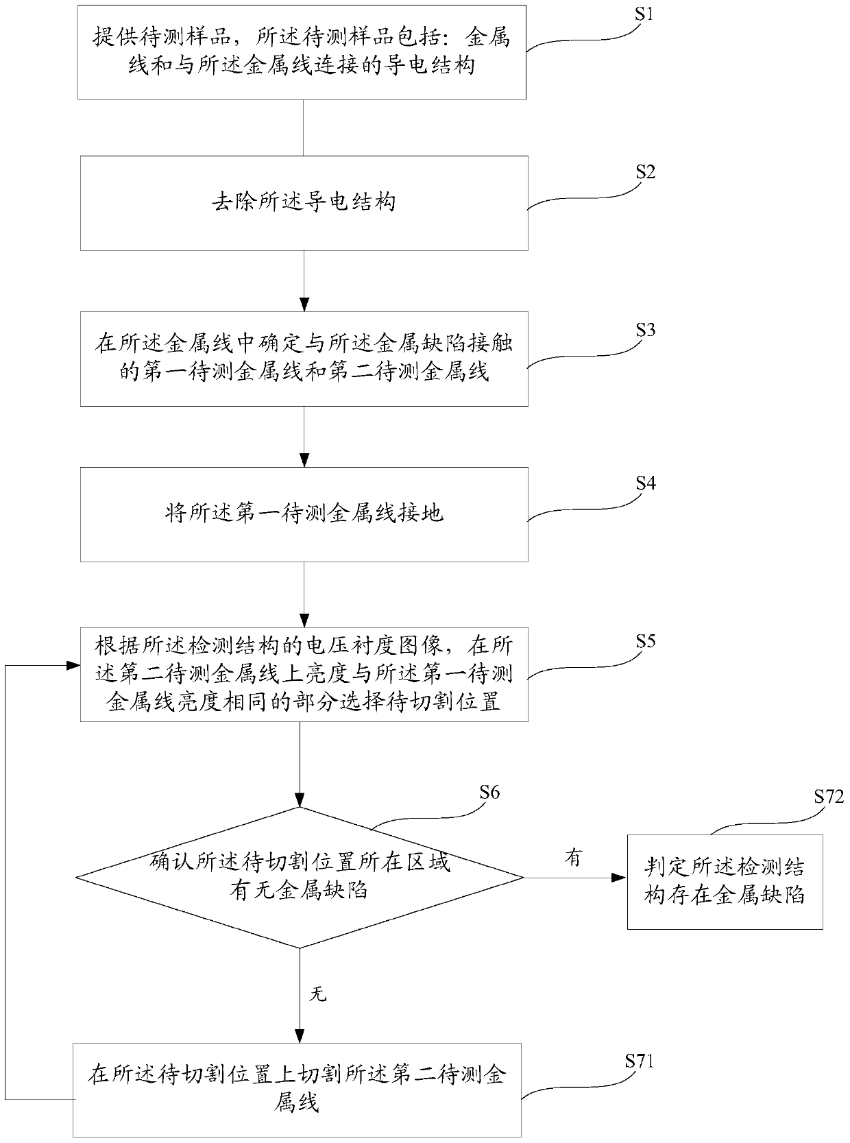
[0031] Such as figure 1 As shown, the embodiment of the present invention provides a method for forming a metal defect detection structure, including:

[0032] Step S1: providing a sample to be tested, the sample to be tested includes: a metal wire and a conductive structure connected to the metal wire;

[0033] Step S2: removing the conductive structure;

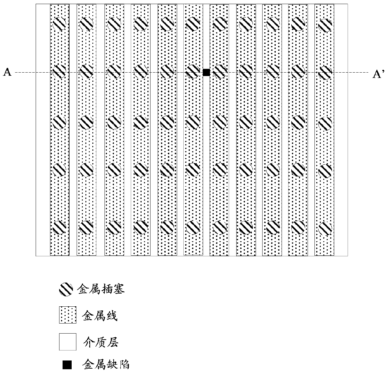
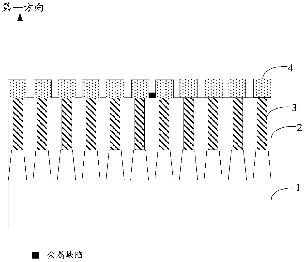
[0034] Step S3: determining a first metal line to be tested and a second metal line to be tested in contact with the metal defect among the metal lines;

[0035] Step S4: grounding the first metal wire to be tested.

[0036] As a specific embodiment, the conductive structure may include: a metal plug, and the sample to be tested may also include: a substrate and a dielectric layer; t...


PUM

PropertyMeasurementUnit
lengthaaaaaaaaaa

Abstract

The invention relates to a metal defect detection method and a detection structure forming method. The metal defect detection structure forming method comprises the steps of providing a sample to be detected, wherein the sample to be detected comprises a metal wire and a conductive structure connected with the metal wire; removing the conductive structure; determining a first metal wire to be detected and a second metal wire to be detected, which are contacted with a metal defect, in the metal wire; and enabling the first metal wire to be detected to be grounded. According to the technical scheme, detection is not directly performed on the original structure of the sample to be detected at which the metal defect is located, the original structure of the sample to be detected is broken to newly establish a new detection structure, and the detection structure can avoid interference brought about by the original structure for detection. On the newly established detection structure, a detection area in which the metal defect is located is gradually reduced by utilizing a voltage contrast image, and the metal defect detection efficiency is improved.

Description

technical field [0001] The invention relates to the field of semiconductors, in particular to a method for detecting metal defects and a method for forming a detection structure. Background technique [0002] With the continuous development of semiconductor integrated circuit device structure, the continuous improvement of process technology and the continuous reduction of device size, more and more defects in semiconductor integrated circuits are invisible. Using traditional defect detection methods to judge its failure mechanism and Finding the physical defect address of a failure is becoming more and more difficult. [0003] For example, in the memory structure, the metal lines used as bit lines are usually larger than 100 microns, while the metal defects generated during the fabrication process are only 100 nanometers, which makes it time-consuming to find the physical location of the metal defects. Using an effective method to locate the physical location of the defect...

Claims


Application Information

Patent Timeline
Patent Type & Authority Patents(China)
IPC IPC(8): H01L21/60
Inventor 殷原梓
Owner SEMICON MFG INT (SHANGHAI) CORP
Why Eureka
Try Eureka