Detection method for blind holes on printed circuit board

A technology for printed circuit boards and detection methods, applied in the directions of printed circuit testing, electronic circuit testing, etc., can solve problems such as inconvenience in use, sheet expansion and shrinkage, and inability to directly inspect, and achieves the effect of improving convenience and overcoming drop.

Active Publication Date: 2017-03-15
万润科技精机(昆山)有限公司
View PDF6 Cites 8 Cited by
  • Summary
  • Abstract
  • Description
  • Claims
  • Application Information

AI Technical Summary

Problems solved by technology

[0004] However, after the printed circuit board has been pressed many times, its board will expand and shrink, resulting in a huge gap between the original design data and the actual measurement data, causing a large number of error messages with deviations in the statistics, resulting in the operator being unable to follow the error messages. Determine whether it is a defect in the manufacturing process. In addition, the printed circuit board needs to clean the residual glue and blackened / brown layer after drilling before performing optical drilling quality inspection. It cannot be inspected directly after drilling. This is in use It is also extremely inconvenient, so our company develops and designs a better blind hole detection method for printed circuit boards to solve the existing technical defects

Method used


Image

  • Detection method for blind holes on printed circuit board
  • Detection method for blind holes on printed circuit board
  • Detection method for blind holes on printed circuit board

Examples


Embodiment Construction

[0041] In order to enable those skilled in the art to better understand the technical solutions in the present application, the technical solutions in the embodiments of the present application will be clearly and completely described below in conjunction with the drawings in the embodiments of the present application. Obviously, the described The embodiments are only some of the embodiments of the present application, but not all of them. Based on the embodiments in this application, all other embodiments obtained by persons of ordinary skill in the art without creative efforts shall fall within the protection scope of this application:

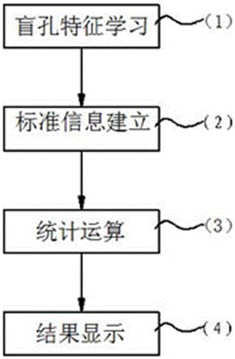
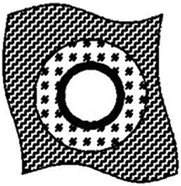
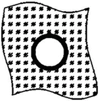
[0042] like Figure 1 to Figure 15 The blind hole detection method of a kind of printed circuit board shown, comprises the following steps:

[0043] (1) Blind hole feature learning: take the actual finished printed circuit board as the first sample a, scan the first sample a and select any image of a blind hole among the plurality of blind ...


PUM


Abstract

The invention discloses a detection method for blind holes on printed circuit board, comprising the following steps: 1) making a sample board according to one real finished product of a printed circuit board; scanning any blind hole image of the plurality of blind holes on the sample board as a learning object; 2) on the basis of the step 1, obtaining the hole positions of the plurality of blind holes on the sample board; using at least one blind hole image characteristics of the sample board to establish the standard information; 3) when the step 2 is completed, scanning a to-be-detected board with the same manufacturing procedures as the sample board; obtaining the to-be-detected information of the plurality of blind holes on the to-be-detected board according to the method in the step 2; and 4) after the deviation statistic amount is calculated, displaying the deviation information in the form of images or charts. According to the invention, the detection method for blinding holes of printed circuit board can overcome the defects of designed data and can be conveniently used.

Description

technical field [0001] The invention relates to the field of printed circuit board production and manufacturing, in particular to a method for detecting blind holes of a printed circuit board. Background technique [0002] In the manufacturing process of printed circuit boards, it is roughly divided into main stations such as inner layer station, pressing station, drilling station, and inspection station in sequence. First, the printed circuit board is developed and etched at the inner layer station, and then Enter the lamination station for blackening / browning treatment, and laminate the printed circuit board multiple times at the lamination station. The laminated printed circuit board then goes to the drilling station for laser drilling, and in the After the drilling is completed, the printed circuit board is cleaned, and finally the printed circuit board is sent to the inspection station for optical drilling quality inspection. [0003] In the quality inspection part of ...

Claims


Application Information

Patent Timeline
Patent Type & Authority Applications(China)
IPC IPC(8): G01R31/28
CPCG01R31/2805
Inventor 郑杰仁郭进顺张家齐
Owner 万润科技精机(昆山)有限公司
Why Eureka
Try Eureka