


Quick Research
Generate reliable direction feasibility study reports for your R&D in just a few steps.

Technical Q&A
Discover and master advanced knowledge NOW. Basics, ideas, possibilities, all at once.

Find Solutions
As an expert in R&D theories, this can generate solutions to your technical problems instantly.

Evaluate Feasibility
Analyze your overall solution with one click, know your potential R&D risks in advance.

Monitor Landscape
Get weekly tech updates, stay abreast of the latest tech innovations and key insights.
A method for preparing large-area photonic crystal scintillators by imprinting technology
A photonic crystal, large-area technology, applied in the field of nuclear radiation measurement, can solve the problem of insufficient depth of nano-imprinting, and achieve the effect of avoiding damage
- Summary
- Abstract
- Description
- Claims
- Application Information
AI Technical Summary
Problems solved by technology
Method used
Image

Examples
Embodiment 1
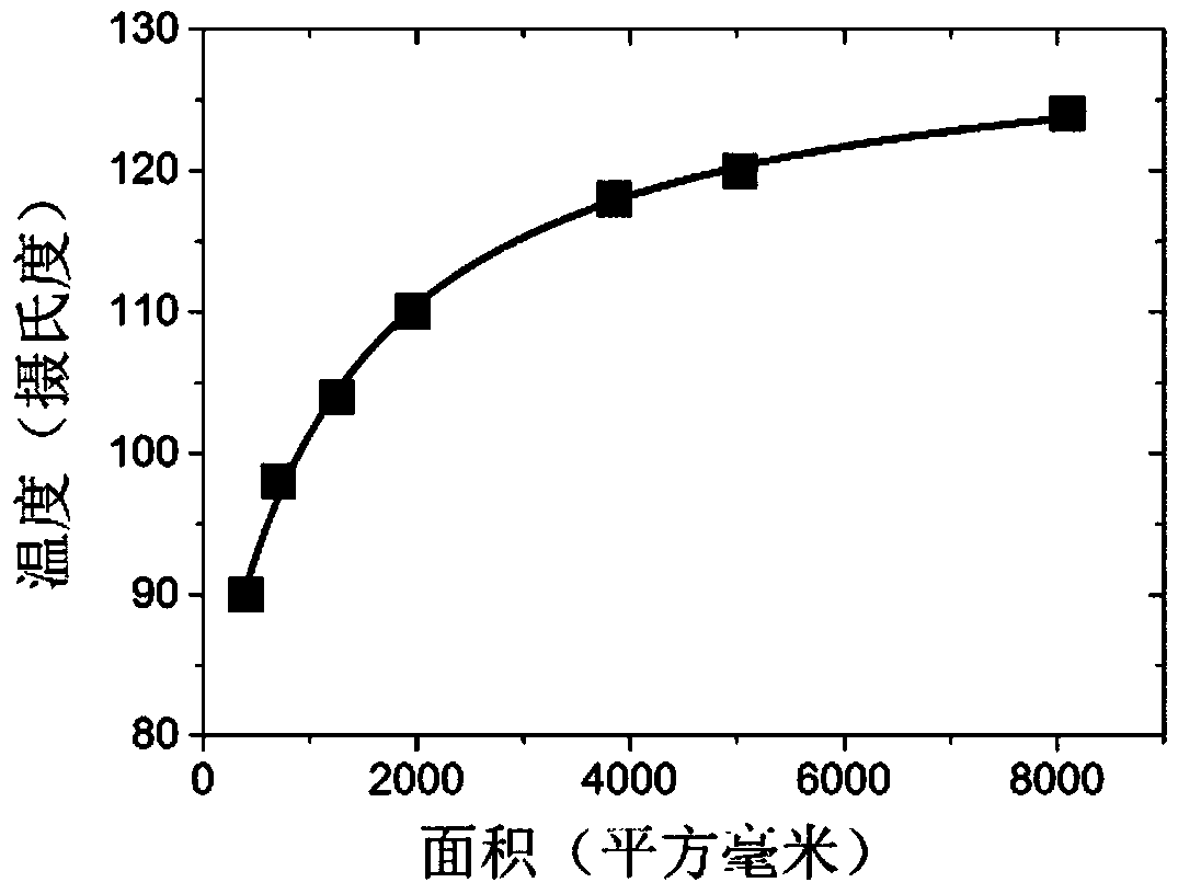
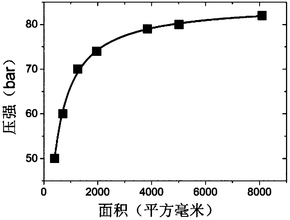
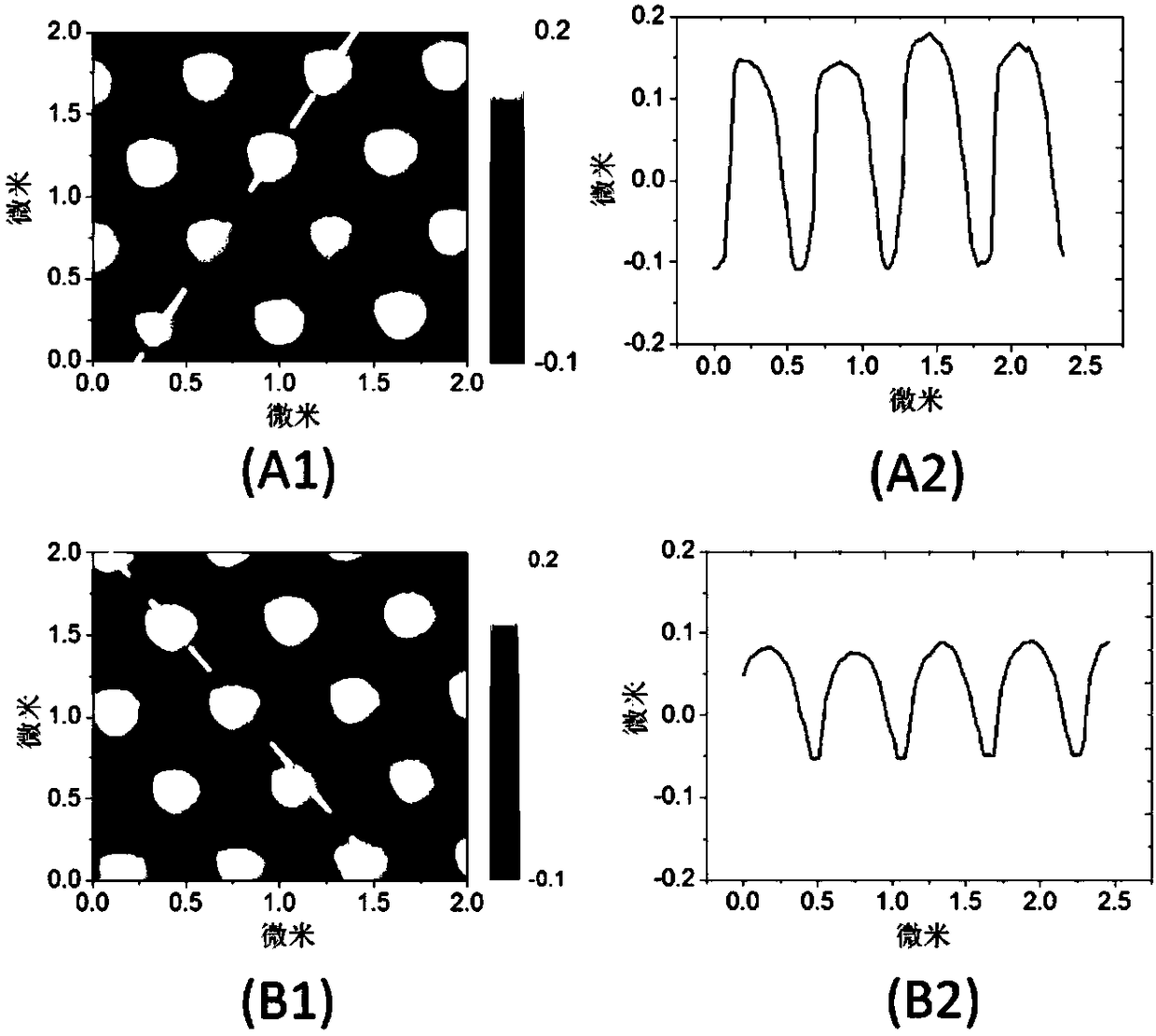
[0032] Photonic crystals were prepared on the surface of EJ212 plastic scintillator (matrix is polyvinyl toluene). The selected template structure was a columnar periodic array with a triangular structure, the period was 600nm, the diameter of the pillar was 300nm, and the height was 300nm. The template had a diameter of 101.6mm, the area is 8103mm 2 The circular template, the template material is silicon.
[0033] The preparation process is as follows:
[0034] Step 1: Cut and polish the EJ212 plastic scintillator to obtain a scintillator with a flat surface. The size is a square with a side length of 120mm and a thickness of 1mm. This size is slightly larger than the size of the template. Prepare two identical samples, one of which is according to The parameters provided by this patent are prepared (sample A), and the other piece is used as a reference sample (sample B), prepared at a lower temperature and pressure, as a control, showing the validity of the parameters in ...
Embodiment 2
[0047] A method for preparing a large-area photonic crystal scintillator by imprinting technology, using the following steps:
[0048] (1) Select a size larger than 400mm 2 The imprint template and the required plastic scintillator of polyvinyltoluene as the matrix material, the imprint template is an array formed by columnar metal units distributed periodically in a triangular structure, the distance between adjacent metal units is 600nm, and the metal units The diameter of the metal unit is 300nm, the height of the metal unit is 300nm, the plastic scintillator and the imprint template are in a complementary structure, and it is a periodic array of holes in a triangular structure. The distance between adjacent holes is 600nm, the hole diameter is 300nm, and the hole depth is 270nm. The area is slightly larger than the imprint template.
[0049] (2) Anti-adhesive treatment is carried out on the template, and the anti-adhesive material perfluorooctyltrichlorosilane is evaporat...
Embodiment 3
[0056] A method for preparing a large-area photonic crystal scintillator by imprinting technology, using the following steps:
[0057] (1) Select a size larger than 400mm 2 The imprint template and the required plastic scintillator with polystyrene as the matrix material, the imprint template is an array of columnar metal units distributed periodically in a triangular structure, the distance between adjacent metal units is 600nm, the metal unit The diameter is 300nm, the height of the metal unit is 300nm, the plastic scintillator and the imprint template have a complementary structure, which is a periodic array of holes in a triangular structure, the distance between adjacent holes is 600nm, the hole diameter is 300nm, the hole depth is 270nm, and the area Slightly larger than the imprint template.
[0058] (2) Anti-adhesive treatment is carried out on the template, and the anti-adhesive material perfluoroquinyltrichlorosilane is vapor-deposited on the surface of the template...
PUM
| Property | Measurement | Unit |
|---|---|---|
| refractive index | aaaaa | aaaaa |
Abstract
Description
Claims
Application Information
 - R&D Engineer
- R&D Manager
- IP Professional
- Industry Leading Data Capabilities
- Powerful AI technology
- Patent DNA Extraction
Browse by: Latest US Patents, China's latest patents, Technical Efficacy Thesaurus, Application Domain, Technology Topic, Popular Technical Reports.
© 2024 PatSnap. All rights reserved.Legal|Privacy policy|Modern Slavery Act Transparency Statement|Sitemap|About US| Contact US: help@patsnap.com