
SRAM type FPGA-based RAM data reliability reinforcement apparatus and method

A technology for strengthening device and reliability, applied in the field of RAM data reliability strengthening device, can solve the problems of reducing memory access speed, increasing hardware overhead, poor reliability, etc., and achieving short error correction time, low error correction cost, and less resource occupation Effect

Active Publication Date: 2017-03-22
HARBIN INST OF TECH
View PDF8 Cites 10 Cited by
  • Summary
  • Abstract
  • Description
  • Claims
  • Application Information

AI Technical Summary

Problems solved by technology

[0006] The present invention aims to solve the problem of high cost and poor versatility of the anti-radiation technology reinforcement method existing in the existing memory reinforcement method; the three-mode redundancy method of the memory will increase hardware overhead, and is not suitable for volume, quality and power cons

Method used


Image

  • SRAM type FPGA-based RAM data reliability reinforcement apparatus and method
  • SRAM type FPGA-based RAM data reliability reinforcement apparatus and method

Examples


specific Embodiment approach 1

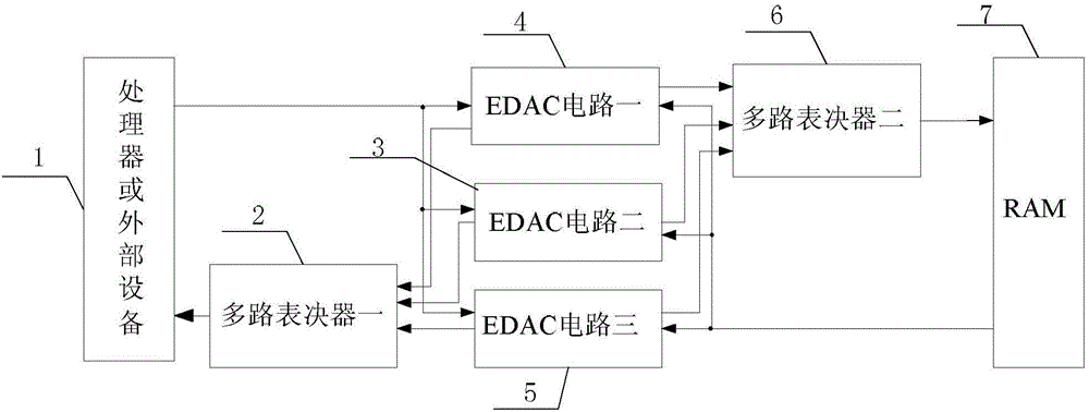
[0041] Specific implementation mode 1. Combination figure 1 Describe this embodiment mode, a kind of RAM data reliability hardening device based on SRAM type FPGA described in this embodiment mode, this device comprises multiplexer one 2, EDAC circuit one 4, EDAC circuit two 3, EDAC circuit three 5 and Multiplexer 2 6;

[0042] The address code signal output terminal and the data signal output terminal of the processor or the external device 1 are simultaneously connected with the address code signal input terminal and the data signal input terminal of the EDAC circuit one 4, the address code signal input terminal and the data signal input terminal of the EDAC circuit two 3 End is connected with the address code signal input end of EDAC circuit three 5 and the data signal input end;

[0043] The address code, read-write control and data signal output terminal of EDAC circuit one 4, the address code, read-write control and data signal output terminal of EDAC circuit two 3, and...

specific Embodiment approach 2

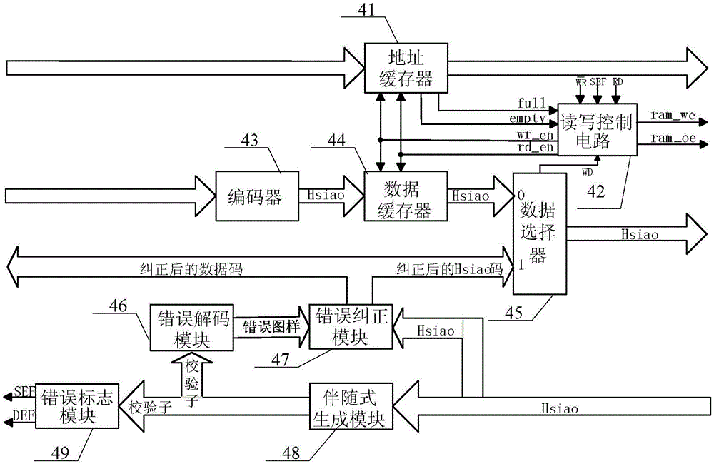
[0046] Specific Embodiment 2. This embodiment is a further description of a RAM data reliability hardening device based on SRAM FPGA described in Specific Embodiment 1. The structures of EDAC circuit one 4, EDAC circuit two 3 and EDAC circuit three 5 Same; EDAC circuit one 4 comprises address buffer 41, read-write control circuit 42, encoder 43, data buffer 44, data selector 45, error decoding module 46, error correction module 47, accompanying formula generating module 48 and error sign Module 49;

[0047] Address buffer 41 is used to receive the address code signal that processor or external device 1 sends; The signal input end of described address buffer 41 is the address code signal input end of EDAC circuit one 4; Send address to multiplexer two 6 code signal;

[0048] The encoder 43 is used to receive the data signal sent by the processor or the external device 1, and send the encoded data signal to the data buffer 44, and the signal input end of the encoder 43 is the d...

specific Embodiment approach 3

[0069] Specific embodiment three, what this embodiment described is a kind of RAM data reliability reinforcement method based on SRAM type FPGA, and the concrete steps of this method are:

[0070] The process of writing the data of processor or external device 1 into RAM7;

[0071] Step 1. Send the address code signal and data signal sent by the processor or external device 1 to EDAC circuit one 4, EDAC circuit two 3 and EDAC circuit three 5 at the same time, and perform three-mode backup of the address code signal and data signal;

[0072] Step 2, EDAC circuit one 4, EDAC circuit two 3 and EDAC circuit three 5 respectively use three encoders to encode the data signal sent by the processor or external device 1 to obtain three-way data encoding, and the encoding is an improved Hamming code ;

[0073] Step 3: Use the multiplexer 2 6 to select two of the three data codes obtained through the EDAC circuit 1 4, EDAC circuit 2 3 and EDAC circuit 3 5 to obtain the correct code, and ...


PUM


Abstract

The invention discloses an SRAM type FPGA-based RAM data reliability reinforcement apparatus and method, relates to an SRAM type FPGA-based on-chip or off-chip RAM data reinforcement apparatus and method, and aims to solve the problems of high anti-radiation process reinforcement expense, high memory triplication redundancy hardware overhead, poor reliability of an EDAC circuit designed based on an SRAM type FPGA, and the like in an existing memory reinforcement method. According to the reinforcement apparatus and method, the encoding/decoding operation of the EDAC circuit is realized by adopting a Hsiao code as an error correction code; a single-error-correcting and double-error-detecting function of data can be realized; the write-back after error data correction is realized in a cache way; and a write address and write data of a processor or a peripheral access dual-port RAM are temporarily stored in an address cache and a data cache. The reinforcement apparatus and method is suitable for the RAM data reliability reinforcement of the SRAM type FPGA.

Description

technical field [0001] The invention relates to a RAM data reliability strengthening device and method based on an SRAM type FPGA. Background technique [0002] With the continuous development of satellite technology and applications, people urgently need to shorten the development cycle of satellites while reducing satellite costs and risks, and small satellite technology has emerged as the times require. [0003] SRAM-type FPGA has been widely used in the aerospace field due to its high integration, good flexibility, repeated programming, low development cost, and high density. However, SRAM-type FPGA is a volatile memory that is vulnerable to single event flips Impact. A single event upset may cause a change in the state of memory data, thereby causing errors in the instructions or data of the on-board computer system, and in severe cases may lead to the collapse of the entire on-board computer system. [0004] In the design of the spaceborne computer system, not only t...

Claims


Application Information

Patent Timeline
IPC IPC(8): G11C29/42
CPCG11C29/42
Inventor 崔秀海王少军沈露马宁彭宇彭喜元
Owner HARBIN INST OF TECH
Learn More