
PCB structure

A technology for printed circuit boards and substrates, applied in the direction of printed circuit components, etc., can solve the problem of discontinuous impedance of signal transmission lines, and achieve the effects of avoiding discontinuous impedance, avoiding noise, and avoiding crosstalk

Inactive Publication Date: 2019-09-13
NOVATEK MICROELECTRONICS CORP
View PDF3 Cites 0 Cited by
  • Summary
  • Abstract
  • Description
  • Claims
  • Application Information

AI Technical Summary

Problems solved by technology

Part of the PCB structure is designed so that the lines of different layers are arranged perpendicular to each other. Although this can reduce the occurrence of coupling effects, if a signal transmission line is densely interleaved with multiple signal transmission lines in another layer, it will also cause problems. It will cause the impedance of the signal transmission line to be discontinuous, so the signal reflection effect will occur

Method used


Image

  • PCB structure
  • PCB structure
  • PCB structure

Examples


Embodiment Construction

[0043] As used throughout this specification (including the claims), the term "coupled" may refer to any connection means, direct or indirect. For example, if it is described in the text that a first device is coupled to a second device, it should be interpreted that the first device can be directly connected to the second device, or the first device can be connected through other devices or some kind of connection means. indirectly connected to the second device. In addition, wherever possible, elements / components / steps using the same reference numerals in the drawings and embodiments represent the same or similar parts. Elements / components / steps using the same symbols or using the same terms in different embodiments can refer to related descriptions.

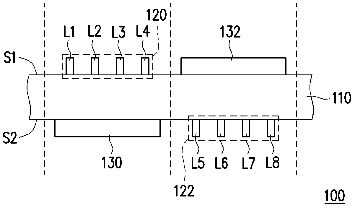
[0044] figure 1 It is a schematic cross-sectional view of a printed circuit board structure 100 according to the first embodiment of the present invention. Please refer to figure 1 The printed circuit board structure 100 i...


PUM


Abstract

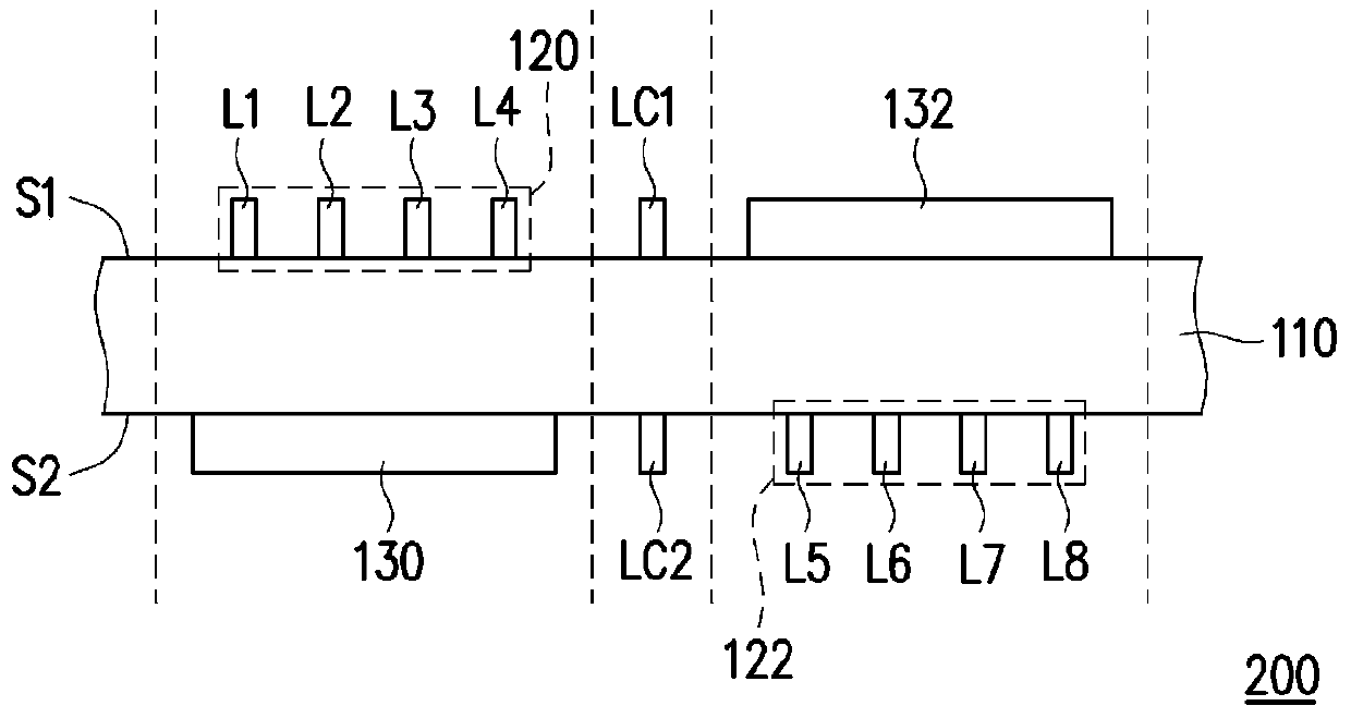
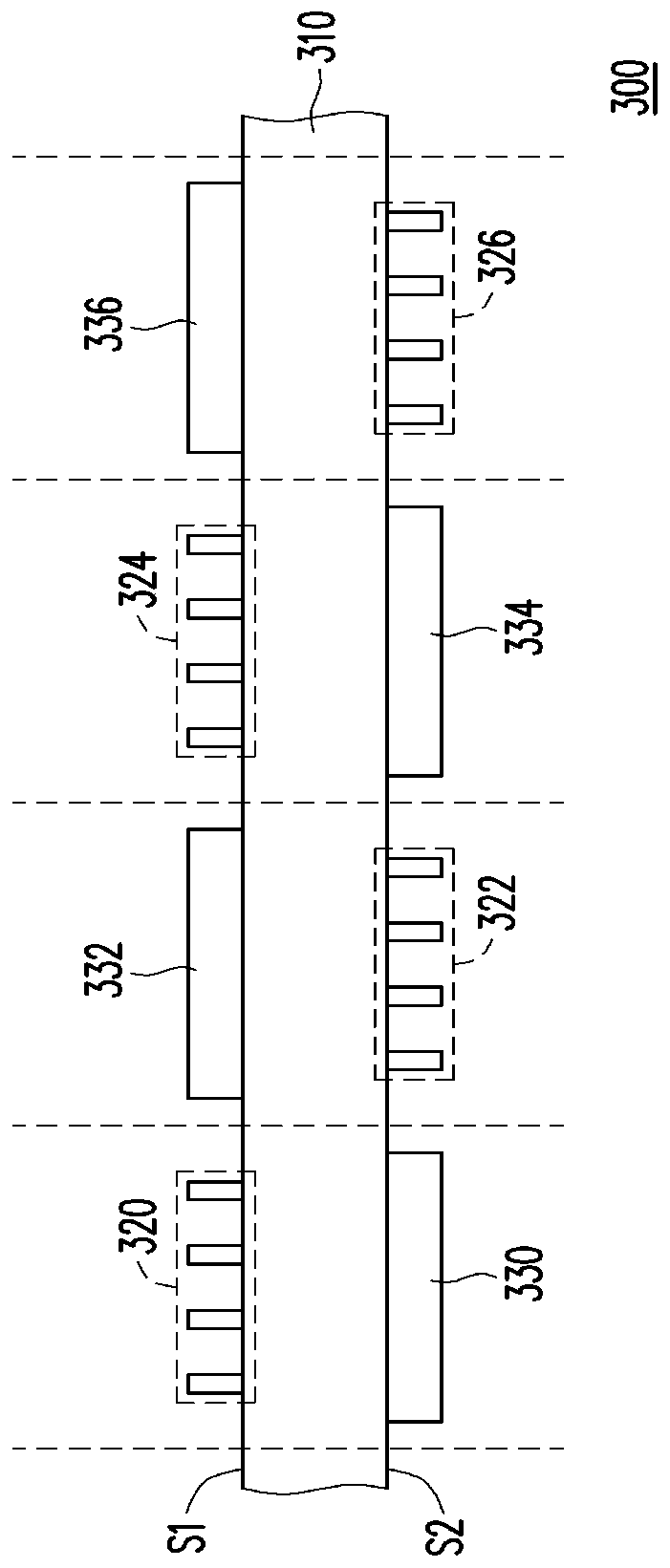
The invention provides a PCB structure which comprises s substrate, a first lead group, a second lead group, a first conductor region and a second conductor region. The substrate comprises a first side and a second side corresponding to the first side, the first lead group is arranged in the first side, and the second lead group is arranged in the second side. The first conductor region is arranged in the second side in an area corresponding to the first lead group and serves as a reference surface of the first lead group. The second conductor region is arranged in the first side in an area corresponding to the second lead group and serves as a reference surface of the second lead group. Thus, the PCB structure can reduce mutual interference among signals transmitted by different lead groups.

Description

technical field [0001] The invention relates to a printed circuit board structure, in particular to a printed circuit board structure for avoiding mutual interference of signals in lines. Background technique [0002] Technology is changing with each passing day. As the processing speed of integrated circuits becomes faster and faster, it is necessary to allow high-speed converted signals to be quickly and smoothly transmitted on printed circuit board (PCB) circuits. As far as the design process of an ideal printed circuit board structure is concerned, it is first necessary to consider signal integrity (Signal integrity) and power integrity (Power integrity) to ensure that the product is fully functional. Due to the limited layout area of ​​the physical circuit, the two signal transmission lines may have electromagnetic coupling effects due to the close wiring, such as crosstalk (crosstalk), that is, the two signal transmission lines generate noise due to capacitive coupling...

Claims


Application Information

Patent Timeline
Patent Type & Authority Patents(China)
IPC IPC(8): H05K1/02
Inventor 林竣义陈郁仁
Owner NOVATEK MICROELECTRONICS CORP
Learn More