


Quick Research
Generate reliable direction feasibility study reports for your R&D in just a few steps.

Technical Q&A
Discover and master advanced knowledge NOW. Basics, ideas, possibilities, all at once.

Find Solutions
As an expert in R&D theories, this can generate solutions to your technical problems instantly.

Evaluate Feasibility
Analyze your overall solution with one click, know your potential R&D risks in advance.

Monitor Landscape
Get weekly tech updates, stay abreast of the latest tech innovations and key insights.
Array substrate
A technology of array substrate and arrangement direction, applied in the field of array substrate, can solve the problems of pixel voltage drop, screen flicker and so on
- Summary
- Abstract
- Description
- Claims
- Application Information
AI Technical Summary
Problems solved by technology
Method used
Image

Examples
Embodiment Construction
[0070] Below in conjunction with accompanying drawing, structural principle and working principle of the present invention are specifically described:
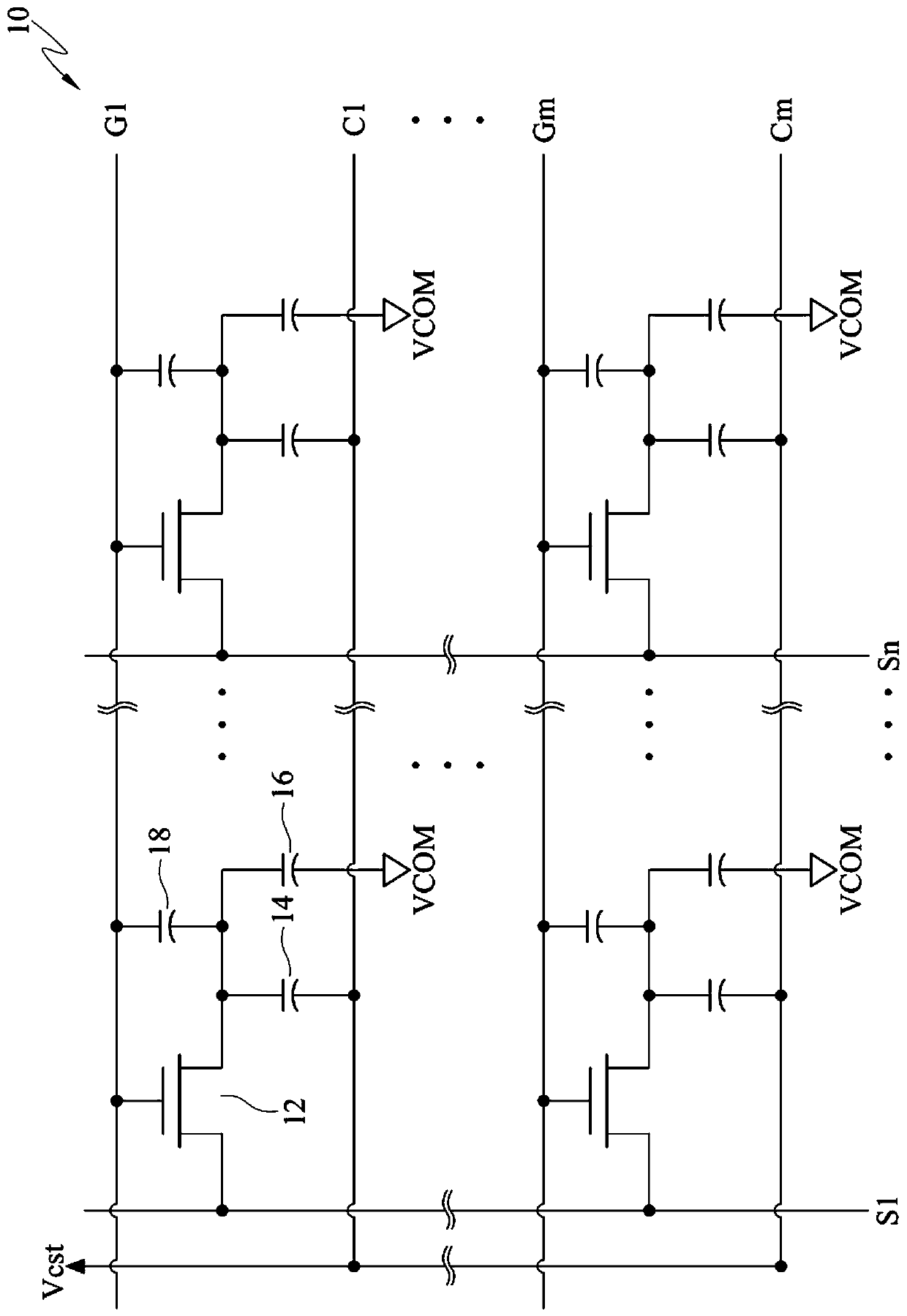
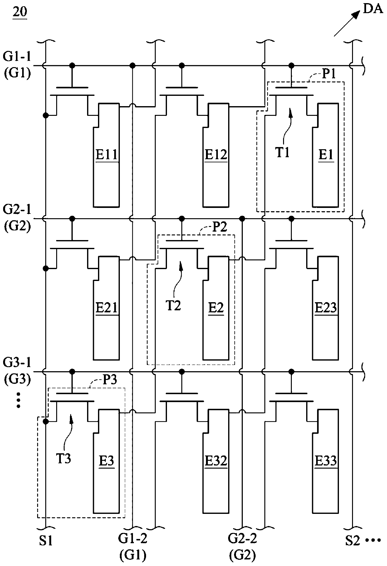
[0071] Please refer to Figure 3A to Figure 3E , Figure 3A It is a schematic diagram of the first embodiment of the array substrate 20 of the present invention. Please refer to Figure 3A , the array substrate 20 includes a plurality of sub-pixels P1, P2, P3, ..., for the convenience of description, Figure 3A Only nine sub-pixels are displayed, and only three sub-pixels are labeled, but this embodiment is not limited thereto.
[0072] The first sub-pixel P1 includes a first active element T1 and a first pixel electrode E1 electrically connected to the first active element T1, and the second sub-pixel P2 includes a second active element T2 and an electrode electrically connected to the second active element T2. The second pixel electrode E2 and the third sub-pixel P3 include a third active element T3 and a third pixel ele...
PUM
 Abstract
Description
Claims
Application Information
 - R&D Engineer
- R&D Manager
- IP Professional
- Industry Leading Data Capabilities
- Powerful AI technology
- Patent DNA Extraction
Browse by: Latest US Patents, China's latest patents, Technical Efficacy Thesaurus, Application Domain, Technology Topic, Popular Technical Reports.
© 2024 PatSnap. All rights reserved.Legal|Privacy policy|Modern Slavery Act Transparency Statement|Sitemap|About US| Contact US: help@patsnap.com