Unlock instant, AI-driven research and patent intelligence for your innovation.

Array substrate, manufacturing method thereof, mask plate, and display device

A technology for array substrates and base substrates, applied in semiconductor/solid-state device manufacturing, instruments, semiconductor devices, etc., can solve problems such as poor dark lines of display devices, and achieve the effects of avoiding dark line defects, solving dark line defects, and avoiding breakage

Active Publication Date: 2019-12-24
BOE TECH GRP CO LTD +1
View PDF4 Cites 0 Cited by
  • Summary
  • Abstract
  • Description
  • Claims
  • Application Information

AI Technical Summary

Problems solved by technology

[0006] In order to solve the problem that the display device is prone to defective dark lines, the present invention provides an array substrate and a manufacturing method thereof, a mask plate, and a display device

Method used


Image

  • Array substrate, manufacturing method thereof, mask plate, and display device
  • Array substrate, manufacturing method thereof, mask plate, and display device
  • Array substrate, manufacturing method thereof, mask plate, and display device

Examples


Embodiment Construction

[0068] In order to make the purpose, technical solutions and advantages of the present invention clearer, the present invention will be further described in detail below in conjunction with the accompanying drawings. Obviously, the described embodiments are only some of the embodiments of the present invention, rather than all of them. Based on the embodiments of the present invention, all other embodiments obtained by persons of ordinary skill in the art without making creative efforts belong to the protection scope of the present invention.

[0069] Please refer to figure 2 , which shows a schematic structural diagram of an array substrate 1 provided by an embodiment of the present invention, see figure 2 , the array substrate 1 includes: a base substrate 11 , and a display unit 12 disposed on the base substrate 11 . Wherein, the base substrate 11 may be a transparent substrate, which may specifically be a substrate made of a light-guiding and non-metallic material with a...


PUM


Abstract

The invention discloses an array substrate, a manufacturing method thereof, a mask plate and a display device, and belongs to the technical field of display. The array substrate comprises: a substrate, and a pixel electrode, a gate electrode, a gate insulating layer, a source and drain electrode layer, a passivation layer and a pixel connecting line, which are arranged on the substrate in sequence, the source and drain electrode layer comprises a source electrode and a drain electrode, a first porous structure is arranged on the gate insulating layer, a second porous structure is arranged at a part located in the first porous structure of the passivation layer, a drain electrode through hole is formed in a part located at the outside of the second porous structure of the passivation layer, a side wall of the second porous structure is not in contact with the side wall of the first porous structure, and the pixel connecting line is used for connecting the pixel electrode with the drain electrode through the second porous structure. The array substrate disclosed by the invention solves the problem that the display device is prone to poor concealed wiring, and achieves the effect of avoiding the poor concealed wiring of the display device. The array substrate disclosed by the invention is applied to the display device.

Description

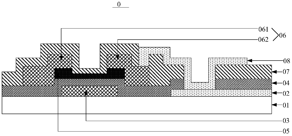
technical field [0001] The present invention relates to the field of display technology, in particular to an array substrate, a manufacturing method thereof, a mask plate, and a display device. Background technique [0002] Liquid crystal display device (English: Liquid Crystal Display; abbreviation: LCD) is a widely used display device. Its main component is a liquid crystal panel. The liquid crystal between the color filter substrates and the array substrate are provided with thin film transistors (English: (Thin Film Transistor; TFT for short), and the LCD generates an electric field through the common electrode and the pixel electrode connected to the TFT to control the deflection of the liquid crystal and realize image display. [0003] Please refer to figure 1 , which shows a schematic structural diagram of an array substrate 0 provided in the related art, see figure 1 , the array substrate 0 includes: a base substrate 01 and a pixel electrode 02, a gate 03, a gate i...

Claims


Application Information

Patent Timeline
Patent Type & Authority Patents(China)
IPC IPC(8): H01L27/12H01L21/77G02F1/1362
CPCG02F1/1362H01L21/77H01L27/1214H01L27/1244H01L27/1259H01L2021/775
Inventor 万云海杨成绍姜涛唐新阳
Owner BOE TECH GRP CO LTD