Shift register and display device provided therewith
一种移位寄存器、电位的技术,应用在静态存储器、数字存储器信息、仪器等方向,能够解决异常动作和消耗电力增大等问题
- Summary
- Abstract
- Description
- Claims
- Application Information
AI Technical Summary
Problems solved by technology
Method used
Image
Examples
no. 1 approach >
[0105]
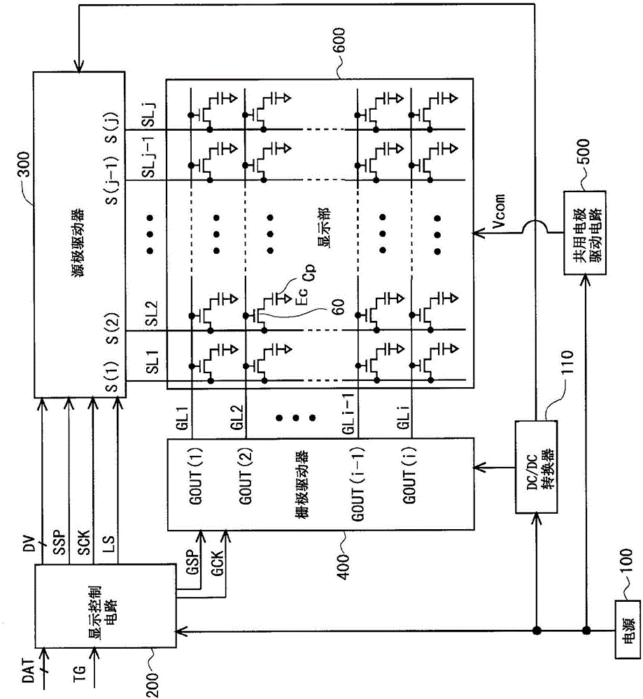
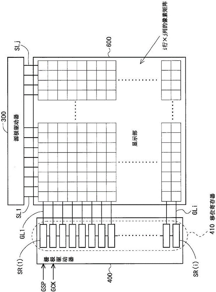
[0106] figure 2 It is a block diagram showing the overall configuration of the active matrix liquid crystal display device according to the first embodiment of the present invention. Such as figure 2 As shown, the liquid crystal display device includes: a power supply 100; a DC / DC converter 110; a display control circuit 200; a source driver (video signal line driving circuit) 300; a gate driver (scanning signal line driving circuit) 400; a drive circuit 500 ; and a display section 600 . In addition, in this embodiment, the gate driver 400 and the display unit 600 are formed on the same substrate (the TFT substrate which is one of the two substrates constituting the liquid crystal panel).
[0107] In the display part 600, there are formed: a plurality of (j) source bus lines (video signal lines) SL1˜SLj; a plurality (i) of gate bus lines (scanning signal lines) GL1˜GLi; The intersections of the bus lines SL1 to SLj and the plurality of gate bus lines GL1 to GLi...
no. 2 approach >
[0143] A second embodiment of the present invention will be described. In addition, only the points of difference from the first embodiment described above will be described.
[0144]
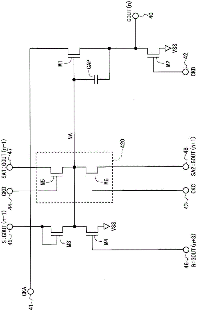
[0145] The overall configuration is the same as that in the above-mentioned first embodiment (refer to figure 2 ) are the same, therefore, the description is omitted. Figure 13 It is a block diagram showing the structure of the shift register 410 in the gate driver 400 in this embodiment. In the first embodiment described above, the scan signal output from the preceding stage is supplied as the set signal S to the constituent circuits SR of each stage. On the other hand, in the present embodiment, the scan signal output from the second preceding stage is supplied as the set signal S to each stage configuration circuit SR. That is, if Figure 14 As shown, for any stage (here set as the nth stage), the scan signal GOUT(n-1) output from the previous stage SR(n-1) is provided as the first c...
no. 3 approach >
[0162]
[0163] A third embodiment of the present invention will be described. The overall configuration is the same as that in the above-mentioned first embodiment (refer to figure 2 ) Likewise, therefore, the description is omitted. The configuration of the shift register 410 in the gate driver 400 is such that a configuration circuit SR of each stage is provided with an initialization signal (a signal for initializing the internal state of the configuration circuit SR of each stage immediately after the vertical scanning period starts) PS It is different from the above-mentioned second embodiment in that an input terminal for receiving a clear signal (a signal for clearing the internal state of each stage configuration circuit SR at the end of the vertical scanning period) CLR. That is, if Figure 19 As shown, the stage configuration circuit SR in this embodiment is provided with: an input terminal for receiving the first clock CKA; an input terminal for receiving the ...
PUM
 Abstract
Description
Claims
Application Information
 - R&D
- Intellectual Property
- Life Sciences
- Materials
- Tech Scout
- Unparalleled Data Quality
- Higher Quality Content
- 60% Fewer Hallucinations
Browse by: Latest US Patents, China's latest patents, Technical Efficacy Thesaurus, Application Domain, Technology Topic, Popular Technical Reports.
© 2025 PatSnap. All rights reserved.Legal|Privacy policy|Modern Slavery Act Transparency Statement|Sitemap|About US| Contact US: help@patsnap.com


