Method for manufacturing multilayer electronic component

A technology for electronic components and manufacturing methods, which is applied in the direction of multilayer capacitors, coil manufacturing, and components of fixed capacitors, etc., can solve problems such as difficulty in suppressing step differences, and achieve the effect of realizing cost reduction and shortening printing time.

Active Publication Date: 2017-05-10
MURATA MFG CO LTD
View PDF7 Cites 3 Cited by
  • Summary
  • Abstract
  • Description
  • Claims
  • Application Information

AI Technical Summary

Problems solved by technology

Therefore, in the manufacturing method disclosed in Patent Document 1, there is a problem that it is difficult to suppress the occurrence of steps due to the inability to fill the insulating paste with a narrow line wid

Method used


Image

  • Method for manufacturing multilayer electronic component
  • Method for manufacturing multilayer electronic component
  • Method for manufacturing multilayer electronic component

Examples


Embodiment approach 1

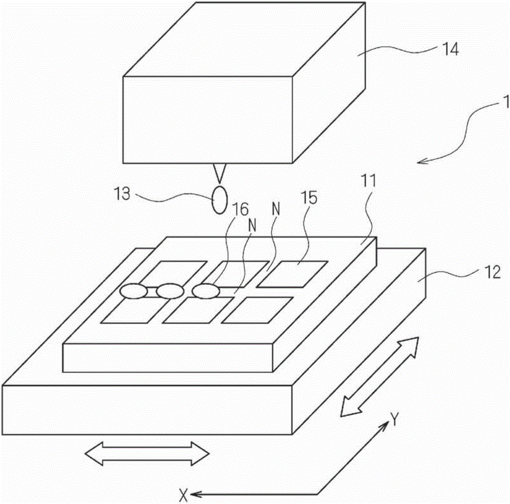
[0033] figure 1 It is a schematic diagram which shows the structure of the printing apparatus used for the manufacturing method of the laminated electronic component which concerns on Embodiment 1 of this invention. figure 1 In the example of , the insulating paste 16 is supplied to the region N between the adjacent internal electrodes 15 of the workpiece using the inkjet method as the printing method.

[0034] Such as figure 1 As shown, the printing apparatus 1 includes a stage 12 on which a workpiece 11 as an object to be printed can be mounted. The stage 12 has a mechanism capable of moving in the left-right direction (X-axis direction) and front-rear direction (Y-axis direction), and can change its positional relationship with the inkjet head 14 provided on the upper part of the workpiece 11 to drop ink droplets 13 . Therefore, ink droplets 13 can be dropped on desired positions of the workpiece 11 mounted on the stage 12 .

[0035] Of course, it is not limited to th...

Embodiment approach 2

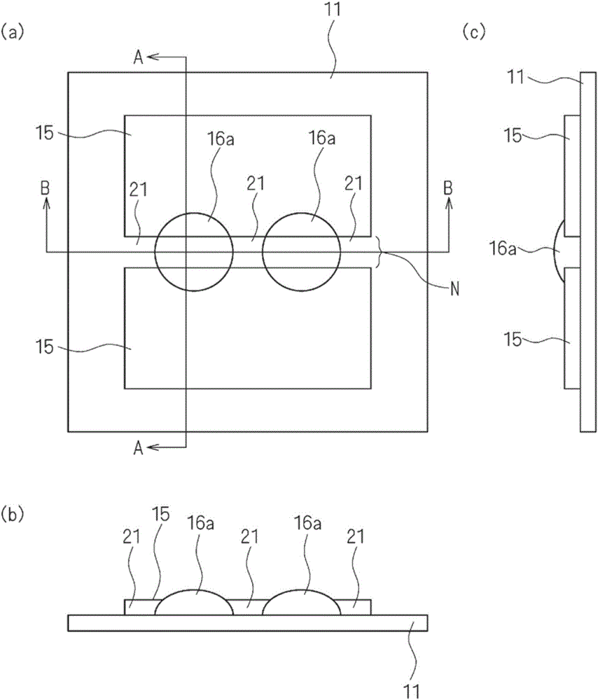
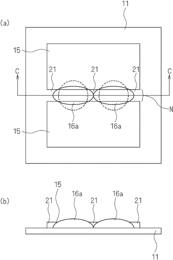
[0053] In the method of manufacturing a laminated electronic component according to Embodiment 2 of the present invention, the steps of producing one ceramic green sheet 11 are the same as those in Embodiment 1, and thus detailed description will be omitted by denoting the same reference numerals. The second embodiment differs from the first embodiment in that the position where the insulating film is formed is changed, and the ceramic green sheets 11 are laminated.

[0054] Figure 5 It is a schematic diagram showing a state where a plurality of ceramic green sheets 11 having insulating films 16a formed at the same positions are stacked in the method of manufacturing a multilayer electronic component according to Embodiment 2 of the present invention. Figure 5 (a) is a plan view showing the state where the insulating film 16a is formed on the ceramic green sheet 11, Figure 5 (b) is Figure 5 E-E sectional view of (a), Figure 5 (c) shows the state after stacking a plural...


PUM


Abstract

Provided is a method for manufacturing a multilayer electronic component that can form insulating parts while suppressing overlapping even when distances between adjacent internal electrodes are small and thus can suppress occurrences of differences in levels during layering. This method for manufacturing the layered electronic component has an insulating part (20) in a region outside of a region wherein internal electrodes (15) are formed in a ceramic green sheet (11). A plurality of insulating films (16a) are formed by supplying insulating paste (16) while keeping a prescribed gap open in regions between adjacent internal electrodes (15) such that the internal electrodes (15) partially overlap. The plurality of insulating films (16a) are made to flow by layering and pressing ceramic green sheets (11) on which the plurality of insulating films (16a) have been formed, and the plurality of insulating films (16a) form the insulating part (20) as a unit in regions outside of the regions where the internal electrodes (15) are formed.

Description

technical field [0001] The present invention relates to a method of manufacturing a laminated electronic component capable of increasing the effective area of ​​internal electrodes during lamination and suppressing a level difference generated in a ceramic laminate. Background technique [0002] In recent years, it has become increasingly difficult to make the thickness of ceramic laminates uniform in accordance with demands for higher functionality, miniaturization, and thinner thickness of electronic devices. For example, in the case of stacking multiple ceramic green sheets, the thickness at the time of stacking varies depending on the positions where conductive films and resistive body films constituting capacitors, resistors, inductors, varistors, filters, etc. are formed. The difference is large, which causes the step difference generated in the ceramic laminate to become larger. [0003] Therefore, for example, Patent Document 1 discloses a method of manufacturing a ...

Claims


Application Information

Patent Timeline
IPC IPC(8): H01G4/30H01F41/12H01G4/12
CPCH01F41/12H01G4/12H01G4/30
Inventor 后藤诚治
Owner MURATA MFG CO LTD
Why Eureka
Try Eureka