Preparation method of heterogeneous Ge-based plasmonic pin diode applied to sleeve antenna

A sleeve antenna and diode technology, which is applied in semiconductor/solid-state device manufacturing, semiconductor devices, electrical components, etc., can solve the problems of low integration, large injection dose and energy, and incompatibility, so as to improve injection efficiency and current, The effect of increasing the breakdown voltage

Inactive Publication Date: 2020-08-28
XIAN UNIV OF SCI & TECH
View PDF2 Cites 0 Cited by
  • Summary
  • Abstract
  • Description
  • Claims
  • Application Information

AI Technical Summary

Problems solved by technology

[0003] The materials used in the pin diodes used in plasma reconfigurable antennas at home and abroad are all bulk silicon materials. This material has the problem of low carrier mobility in the intrinsic region, which affects the carrier concentration in the intrinsic region of the pin diode, which in turn affects its Solid-state plasma concentration; and the P region and N region of the structure are mostly formed by implantation process, which requires a large implant dose and energy, high requirements on equipment, and is not compatible with existing processes; and the use of diffusion process, although the junction Deeper, but at the same time, the area of ​​the P region and the N region is large, the integration degree is low, and the doping concentration is uneven, which affects the electrical performance of the pin diode, resulting in poor controllability of the solid-state plasma concentration and distribution

Method used


Image

  • Preparation method of heterogeneous Ge-based plasmonic pin diode applied to sleeve antenna
  • Preparation method of heterogeneous Ge-based plasmonic pin diode applied to sleeve antenna
  • Preparation method of heterogeneous Ge-based plasmonic pin diode applied to sleeve antenna

Examples


Embodiment 1

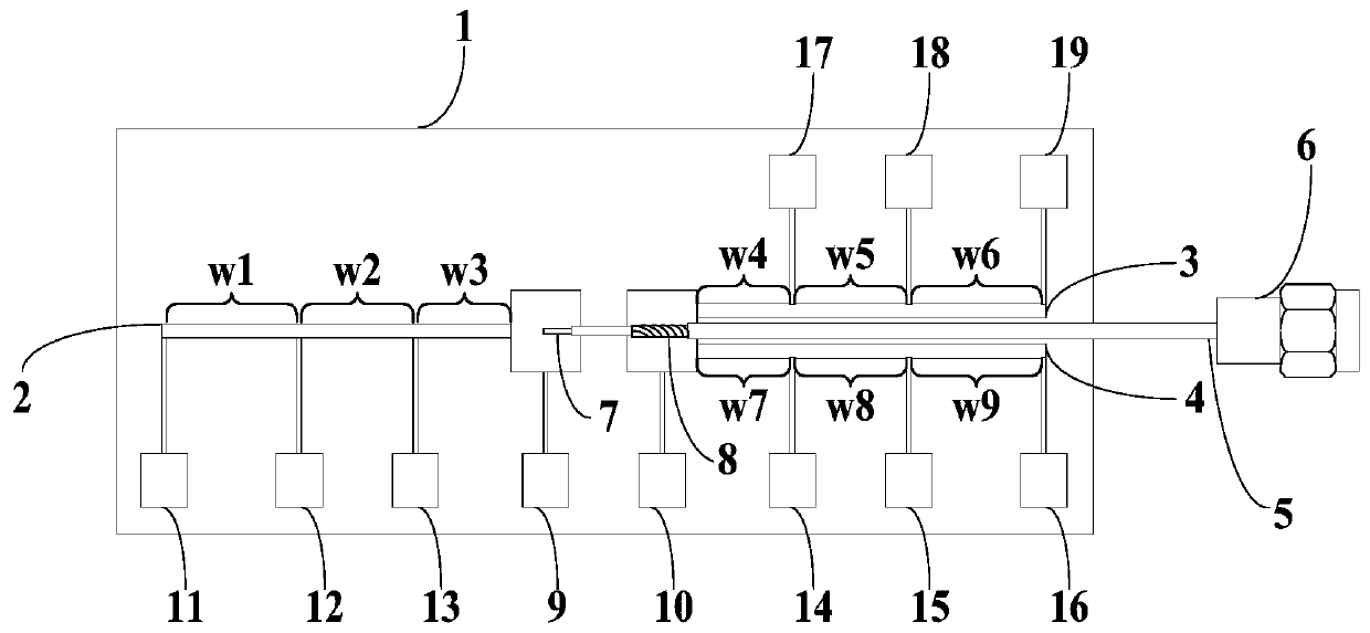
[0058] See figure 1 , figure 1 It is a structural schematic diagram of a reconfigurable sleeve antenna according to an embodiment of the present invention. The sleeve antenna includes: a semiconductor substrate (1), a pin diode antenna arm (2), a first pin diode sleeve (3), a second pin diode sleeve (4), a coaxial feeder (5), a direct current Bias lines (9, 10, 11, 12, 13, 14, 15, 16, 17, 18, 19);

[0059] The pin diode antenna arm (2), the first pin diode sleeve (3), the second pin diode sleeve (4) and the DC bias line (9, 10, 11, 12, 13 , 14, 15, 16, 17, 18, 19) are all fabricated on the semiconductor substrate (1); the pin diode antenna arm (2) and the first pin diode sleeve (3) and the The second pin diode sleeve (4) is connected through the coaxial feeder (5), the inner core wire (7) of the coaxial feeder (5) is connected to the pin diode antenna arm (2) and the coaxial The outer conductor (8) of the feeder (5) is connected to the first pin diode sleeve (3) and the se...

Embodiment 2

[0107] See Figure 5a-Figure 5r , Figure 5a-Figure 5r It is a schematic diagram of another method for preparing a heterogeneous Ge-based plasmonic pin diode according to an embodiment of the present invention. On the basis of the above-mentioned embodiment 1, take the preparation of a GeOI-based solid-state plasma pin diode with a channel length of 22nm (the length of the solid-state plasma region is 100 microns) as an example to describe in detail, and the specific steps are as follows:

[0108] Step 1, substrate material preparation steps:

[0109] (1a) if Figure 5a As shown, the (100) crystal orientation is selected, the doping type is p-type, the doping concentration is a GeOI substrate 101 of 1014 cm-3, and the thickness of the top layer Ge is 50 μm;

[0110] (1b) if Figure 5b As shown, a first SiO2 layer 201 with a thickness of 40nm is deposited on a GeOI substrate by chemical vapor deposition (Chemical vapor deposition, CVD for short);

[0111] (1c) Depositing a...

Embodiment 3

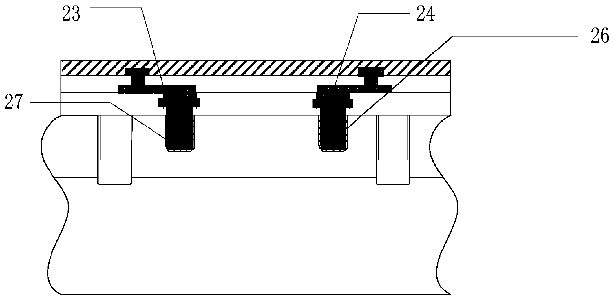
[0138] Please refer to Figure 6 , Figure 6 It is a schematic structural diagram of another heterogeneous Ge-based plasmonic pin diode according to an embodiment of the present invention. The heterogeneous Ge-based plasmonic pin diode employs the above-mentioned as figure 2 The preparation method shown is made, specifically, the Ge-based plasma pin diode is prepared and formed on the GeOI substrate 301, and the P region 304, the N region 305 of the pin diode and the lateral position between the P region 304 and the N region 305 The I regions in between are located in the top layer Ge302 of the GeOI substrate. Wherein, the pin diode can be isolated by STI deep trenches, that is, an isolation trench 303 is provided outside the P region 304 and the N region 305, and the depth of the isolation trench 303 is greater than or equal to the thickness of the top layer Ge302.


PUM


Abstract

The invention relates to a preparation method of a heterogeneous Ge-based plasma pin diode applied to a sleeve antenna. The preparation method comprises the steps of selecting a GeOI substrate of one crystal orientation and arranging an isolation area in the GeOI substrate; etching the GeOI substrate to form a P-type groove and an N-type groove, wherein the depths of the P-type groove and the N-type groove are smaller than the thickness of top-layer Ge of the GeOI substrate; filling the P-type groove and the N-type groove and forming a P-type active area and an N-type active area in the top-layer Ge of the GeOI substrate by adopting ion implantation; and forming a lead on the GeOI substrate to complete preparation of the heterogeneous Ge-based plasma pin diode. The high-performance Ge-based plasma pin diode suitable for forming a solid-state plasma antenna can be prepared and provided by adopting a deep groove isolation technology and an ion implantation technology.

Description

technical field [0001] The invention relates to the technical field of semiconductor device manufacturing, in particular to a method for preparing a heterogeneous Ge-based plasma pin diode applied to a sleeve antenna. Background technique [0002] In modern communication and remote sensing systems, sleeve antennas have been widely used due to their good broadband characteristics. In recent years, the theoretical research of the sleeve antenna has been paid more and more attention. In addition, reconfigurable antennas, especially frequency reconfigurable antennas, can work at multiple frequencies, which greatly expands the application range of antennas, and has always been one of the focuses of research in the field of antennas at home and abroad. [0003] The materials used in the pin diodes used in plasma reconfigurable antennas at home and abroad are all bulk silicon materials. This material has the problem of low carrier mobility in the intrinsic region, which affects th...

Claims


Application Information

Patent Timeline
Patent Type & Authority Patents(China)
IPC IPC(8): H01L21/329H01L29/868
CPCH01L29/6609H01L29/868
Inventor 李妤晨
Owner XIAN UNIV OF SCI & TECH
Why Eureka
Try Eureka