Array substrate and preparation method thereof, display device

An array substrate, intermediate position technology, applied in semiconductor/solid-state device manufacturing, electrical components, electric solid-state devices, etc., can solve the problems of reduced charging rate of electrodes 14, uneven brightness of display panels, and reduced display effects, etc.

Inactive Publication Date: 2017-05-31
BOE TECH GRP CO LTD +1
View PDF5 Cites 6 Cited by
  • Summary
  • Abstract
  • Description
  • Claims
  • Application Information

AI Technical Summary

Problems solved by technology

[0005] Based on the above, since the resistance on the gate line gradually increases along the direction away from the scanning signal input end, the gate line generates RC Delay (resistance-capacitance delay), such as figure 1 As shown, the waveform of the scanning signal input to the grid line is distorted, that is, when the scanning signal with a normal waveform input from the scanning signal input terminal is transmitted along the extending direction of the grid line, the scanning si

Method used


Image

  • Array substrate and preparation method thereof, display device
  • Array substrate and preparation method thereof, display device
  • Array substrate and preparation method thereof, display device

Examples


Embodiment Construction

[0042] The following will clearly and completely describe the technical solutions in the embodiments of the present invention with reference to the accompanying drawings in the embodiments of the present invention. Obviously, the described embodiments are only some, not all, embodiments of the present invention. Based on the embodiments of the present invention, all other embodiments obtained by persons of ordinary skill in the art without making creative efforts belong to the protection scope of the present invention.

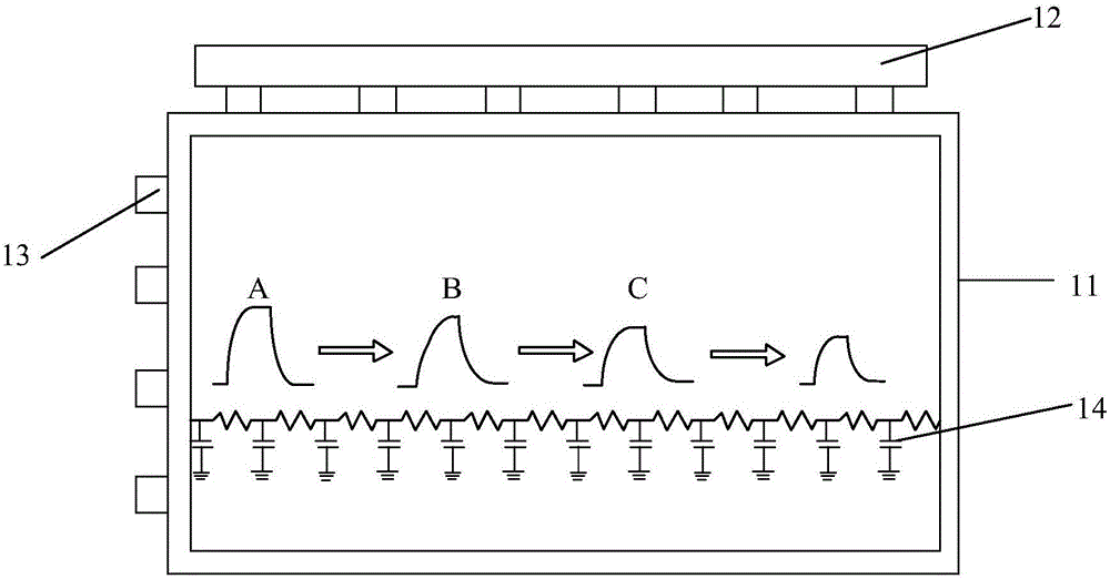
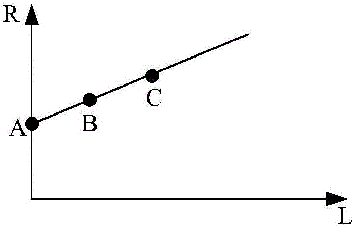
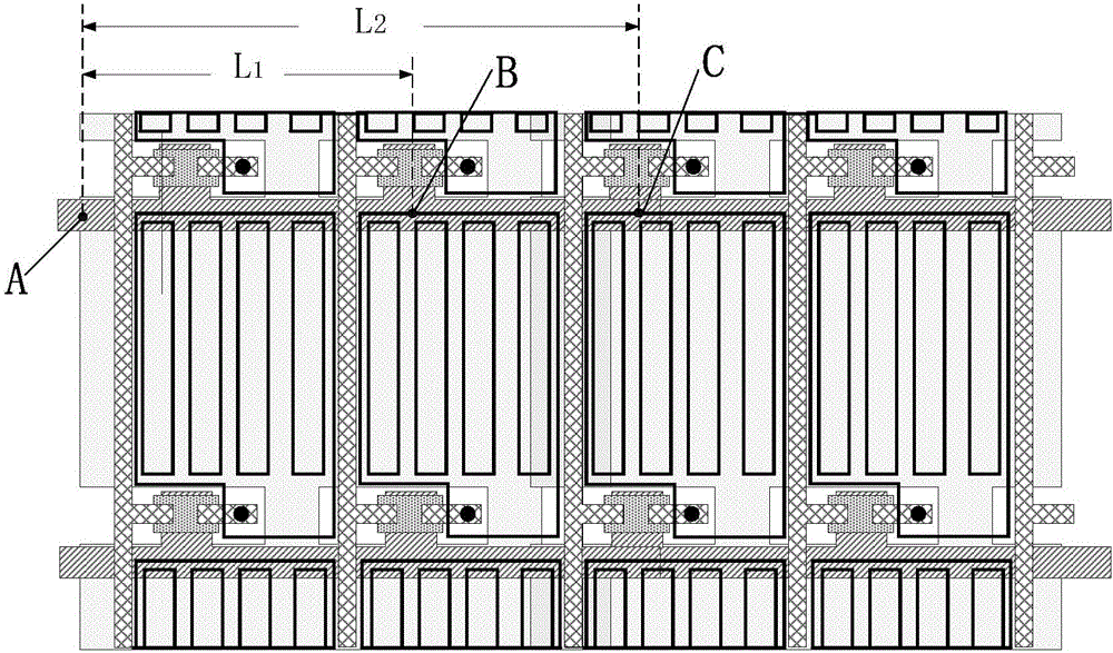
[0043] An embodiment of the present invention provides an array substrate, such as Figure 4 As shown, it includes a gate line 20 arranged on the substrate 10, one end of the gate line 20 is the scanning signal input terminal (connected to the scanning driver 13), and the cross-sectional area of ​​the gate line gradually increases along the direction away from the scanning signal input terminal. Wherein, the grid line cross-section is on the grid line 20 and t...


PUM


Abstract

The invention provides an array substrate and a preparation method of the array substrate, and a display device, and relates to the technical field of display. The invention can reduce the influence of resistance-capacitance delay of a grid line. The array substrate comprises the grid line arranged on the substrate, wherein one end of the grid line is a scanning signal input end, and moves along the direction far from the input end of the scanning signal; area of the cross section of the grid line is gradually increased; or both ends of the grid line are scanning signal input ends, and moves along the middle position of the input end of the scanning signal and the grid line; the area of the cross section of the grid line is gradually increased, wherein the cross section of the grid line is the section face on the grid line perpendicular to the extension direction of the grid line.

Description

technical field [0001] The present invention relates to the field of display technology, in particular to an array substrate, a preparation method thereof, and a display device. Background technique [0002] With the development of display technology, people have higher and higher requirements on the display effect of the display panel. [0003] Such as figure 1 As shown, the display panel 11 is generally driven by a data driver 12 and a scan driver 13 located around it to display. The scan signal of the gate line is input by the scan driver 13 connected to the gate line to control the opening of a row of thin film transistors connected to the gate line, so that the data driver 12 can pass the data line through the open thin film transistor to the electrode 14 of the display panel 11 The voltage signal required for displaying the picture is input to realize the display on the display panel 11 . [0004] Among them, the resistance value of the grid line R=PL / S, P is the re...

Claims


Application Information

Patent Timeline
IPC IPC(8): H01L27/12H01L21/77
Inventor 宫奎刘天真陈程段献学
Owner BOE TECH GRP CO LTD
Why Eureka
Try Eureka