TFT array substrate

An array substrate and array-type technology, applied in optics, instruments, electrical components, etc., can solve the problems of insufficient brightness of even-numbered sub-pixels and insufficient charging of even-numbered sub-pixels, so as to improve display defects, avoid false charging and display, and reduce resistance. The effect of delay tolerance

Inactive Publication Date: 2015-01-14
TCL CHINA STAR OPTOELECTRONICS TECH CO LTD
View PDF4 Cites 28 Cited by
  • Summary
  • Abstract
  • Description
  • Claims
  • Application Information

AI Technical Summary

Problems solved by technology

When the scan lines G1, G2, G3, G4, etc. are turned on sequentially, the even-numbered sub-pixels connected to both sides of each data line are sequentially driven row by row before the odd-numbered sub-pixels, for example, the sub-pixels P12, P13, P22, and P23 are driven sequentially. In the period of the same polarity of the data signal, the sub-pixels driven later are always charged better than the sub-pixels driven first. In this way, P13 is better charged than P12, and P23 is better charged than P22. After sex reversal, the driving sequence remains unchanged, and the even-numbered sub-pixels are still driven first, and then the odd-numbered sub-pixels are driven; The sub-pixels in the even-numbered columns may be insufficiently charged, so that the brightness of the positions corresponding to the sub-pixels in the even-numbered columns is insufficient, and the defect of vertical bright and dark lines is formed from the perspective of the overall display effect.

Method used


Image

  • TFT array substrate
  • TFT array substrate
  • TFT array substrate

Examples


Embodiment Construction

[0033] In order to further illustrate the technical means adopted by the present invention and its effects, the following describes in detail in conjunction with preferred embodiments of the present invention and accompanying drawings.

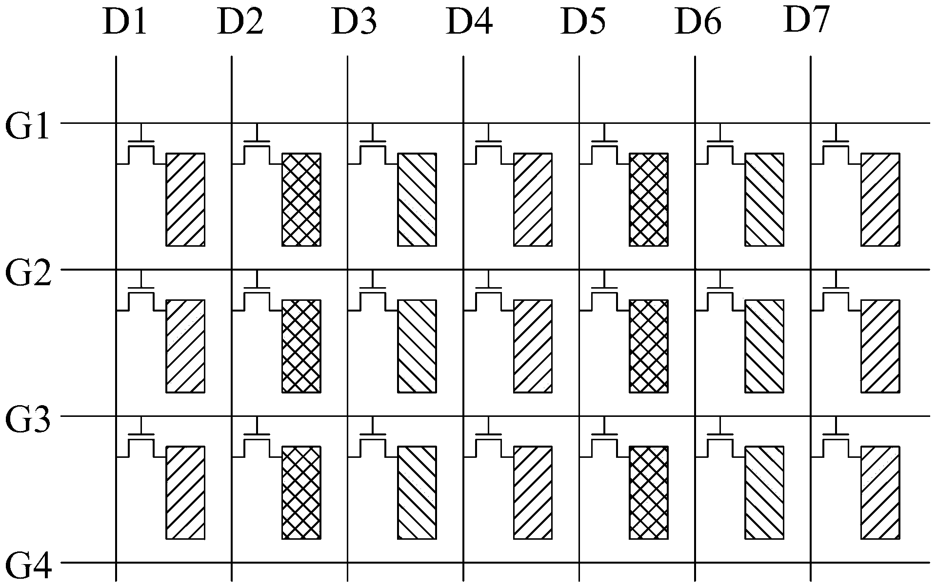
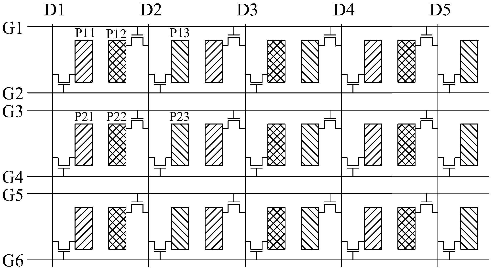
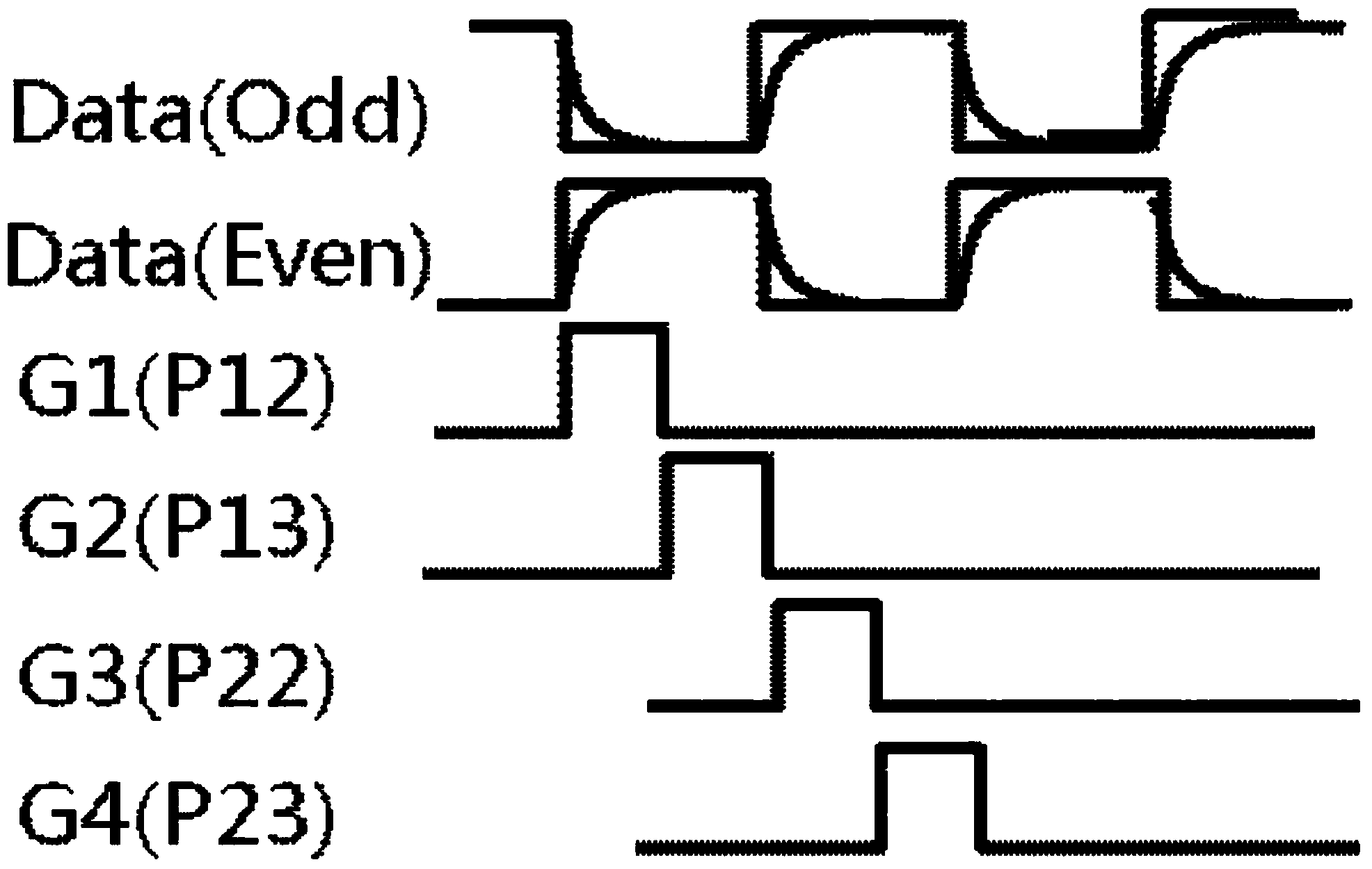
[0034] see Figure 5 , is a schematic diagram of the first embodiment of the TFT array substrate of the present invention. The TFT array substrate includes: a plurality of data lines, such as D1, D2, D3, D4, D5, D6, D7, etc., a plurality of scanning lines, and a plurality of sub-pixels in an array.

[0035] A pair of sub-pixels located between two adjacent data lines in each row of sub-pixels are aligned, and adjacent odd-numbered sub-pixels and even-numbered sub-pixels in each row of sub-pixels are laterally staggered on a plane.

[0036] Each data line is electrically connected to two sub-pixels on the left and right sides of the data line in each row of sub-pixels through TFTs, and provides data signals for the two sub-pixels.

[0037] Co...


PUM


Abstract

The invention provides a TFT array substrate. The sub pixel arraying manner is changed, the sub pixels, with uneven brightness, of the space are arrayed in a staggered manner in the same frame image display period, and the display defects of vertical bright and dark lines are optimized; the entire resistance of a data line can be reduced, resistance-capacitance delay can be reduced, and wrong charge of the tail end of a scanning line or data line is avoided.

Description

technical field [0001] The present invention relates to the field of display technology, in particular to a TFT array substrate. Background technique [0002] In the field of display technology, flat-panel displays such as Liquid Crystal Display (LCD) and Organic Light Emitting Diode (OLED) have gradually replaced CRT displays, and are widely used in LCD TVs, mobile phones, personal digital assistants, digital Cameras, computer or laptop screens, etc. [0003] The display panel is an important part of LCD and OLED. Whether it is an LCD display panel or an OLED display panel, it usually has a thin film transistor (Thin Film Transistor, TFT) array substrate. A plurality of R, G and B sub-pixels arranged in an array, a plurality of scanning lines, and a plurality of data lines are formed on the TFT array substrate. Each sub-pixel receives a scan signal through a corresponding scan line and a data signal through a corresponding data line to display an image. [0004] figure...

Claims


Application Information

Patent Timeline
Patent Type & Authority Applications(China)
IPC IPC(8): G02F1/1362H01L27/32G09G3/36G09G3/32G09G3/3225
CPCG02F1/136286G09G3/3225G09G3/3648H10K59/131G09G3/3614G09G2300/0426G02F1/1368G09G3/3674G09G2300/0408
Inventor 陈彩琴许哲豪
Owner TCL CHINA STAR OPTOELECTRONICS TECH CO LTD
Why Eureka
Try Eureka