Double-sided organic light emitting diode (OLED) display and package method thereof

A display and double-sided technology, applied in the field of double-sided OLED display and its packaging, can solve the problem of damage to the display surface, achieve the effect of reducing the edge width and prolonging the display life

Active Publication Date: 2017-05-31
WUHAN CHINA STAR OPTOELECTRONICS TECH CO LTD
View PDF6 Cites 0 Cited by
  • Summary
  • Abstract
  • Description
  • Claims
  • Application Information

AI Technical Summary

Problems solved by technology

[0005] The present invention provides a double-sided OLED display. The luminescent display part is arranged in a transparent encapsulation case, and the side part of the luminescent display part is bonded to the transparent encapsulation case, which can solve the problem of damage to the display surface caused by smearing sealant on the surface of the luminescent display part. technical problem

Method used


Image

  • Double-sided organic light emitting diode (OLED) display and package method thereof
  • Double-sided organic light emitting diode (OLED) display and package method thereof
  • Double-sided organic light emitting diode (OLED) display and package method thereof

Examples


Embodiment 1

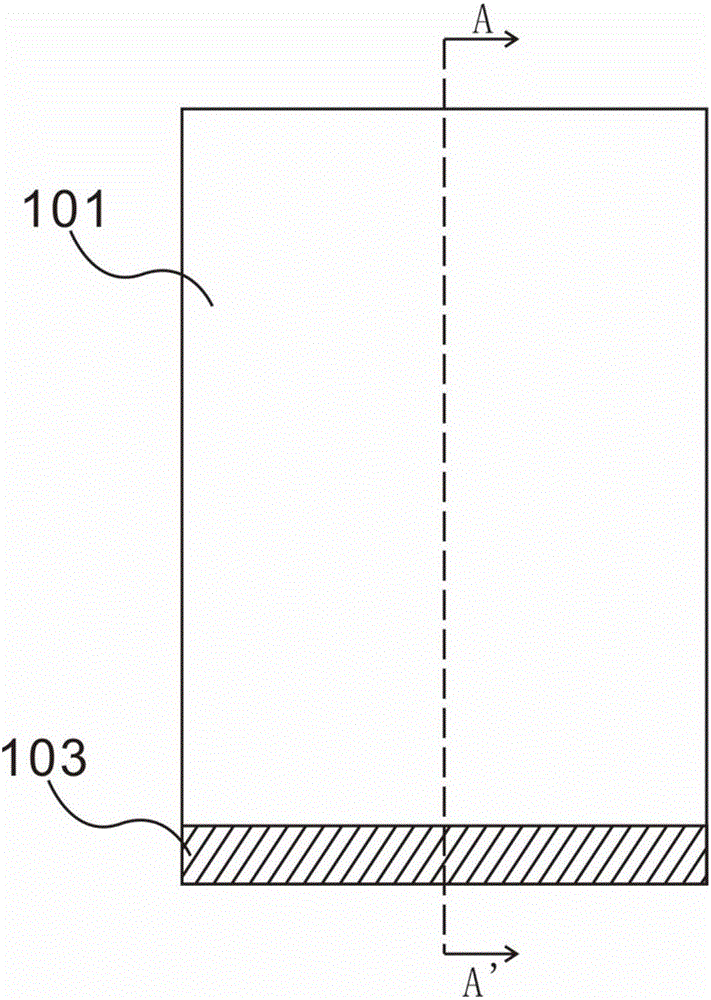
[0051] see figure 1 , is a top view of the double-sided OLED display of the present invention.

[0052] Such as figure 1 As shown, an upper packaging cover 101 is included, and a first light-emitting display part is fixed inside the upper package cover 101. The first light-emitting display part includes a first light-emitting layer and a first light-emitting layer located at the bottom of the first light-emitting layer. The base 103, the end of the first base 103 protrudes from one end of the upper package cover 101, and is used for binding the display control device.

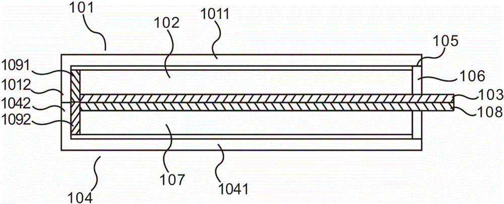
[0053] Such as figure 2 shown, for figure 1 The sectional view along AA' includes an upper package cover 101 and a lower package cover 104, the lower surface of the upper package cover 101 is closely attached to the upper surface of the lower package cover 104, and the upper package cover 101 and the lower package cover 104 are closely attached. The packaging cover 104 is combined to form an accommodating ...

Embodiment 2

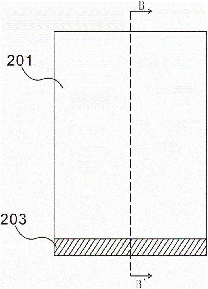
[0061] see image 3 , is a top view of the double-sided OLED display of the present invention.

[0062] Such as image 3 As shown, an upper packaging cover 201 is included, and a first light-emitting display part is fixed inside the upper package cover 201. The first light-emitting display part includes a first light-emitting layer and a first light-emitting layer located at the bottom of the first light-emitting layer. The base 203, the end of the first base 203 protrudes from one end of the upper package cover 201, and is used for binding the display control device.

[0063] Such as Figure 4 shown, for image 3 The sectional view along BB' includes an upper package cover 201 and a lower package cover 204, the lower surface of the upper package cover 201 is closely attached to the upper surface of the lower package cover 204, and the upper package cover 201 and the lower package cover The packaging cover 204 is combined to form an accommodating chamber for accommodating ...

Embodiment 3

[0071] see Figure 5 , is a top view of the double-sided OLED display of the present invention.

[0072] Such as Figure 5 As shown, an upper packaging cover 301 is included, and a first light-emitting display part is fixed inside the upper package cover 301. The first light-emitting display part includes a first light-emitting layer and a first light-emitting layer located at the bottom of the first light-emitting layer. The base 303, the end of the first base 303 protrudes from one end of the upper package cover 301, and is used for binding the display control device.

[0073] Such as Figure 6 shown, for Figure 5 The sectional view along CC' includes an upper package cover 301 and a lower package cover 304, the upper package cover 301 and the lower package cover 304 are fastened together, that is, part or all of the upper package cover 301 is placed in the The inside of the lower packaging cover 304 is described. The combination of the upper packaging cover 301 and the...


PUM


Abstract

The invention provides a double-sided organic light emitting diode (OLED) package structure. The double-sided OLED package structure comprises an upper plate body and a lower plate body, wherein bending structures are arranged at edges of the upper plate body and the lower plate body, and package adhesives are arranged at inner sides of the bending structures so that side parts of a first substrate and a second substrate are respectively and correspondingly connected with the bending structures by the package adhesives. The double-sided LED package structure has the beneficial effects that the package adhesives are arranged at side parts of package covers and are far away from a light emitting surface, so that an organic light emitting layer is free from the damage of a high temperature, and the display lifetime is prolonged; and the side parts of the package covers can be thinned so as to be beneficial for reducing the frame width of a double-sided display.

Description

technical field [0001] The invention relates to the field of display technology, in particular to a double-sided OLED display and a packaging method thereof. Background technique [0002] Organic Light Emitting Diode (OLED) displays are becoming more common, most notably in products such as mobile phones, media players and small entry-level TVs; It has the advantages of wide viewing angle, fast response speed, and flexible preparation; at the same time, when OLED devices work, electrons are injected from the cathode, which requires that the cathode work function be as low as possible, but these metals used as cathodes such as aluminum, magnesium, and calcium etc., are generally live waves, and are easy to react with the infiltrated water vapor, thereby affecting the working life of the OLED device. Therefore, the OLED device needs to be packaged during production to avoid entering water vapor. [0003] With the diversification of electronic products, double-sided display ha...

Claims


Application Information

Patent Timeline
Patent Type & Authority Applications(China)
IPC IPC(8): H01L27/32H01L51/52H01L51/56
CPCH10K59/88H10K59/12H10K50/841H10K71/00
Inventor 唐岳军
Owner WUHAN CHINA STAR OPTOELECTRONICS TECH CO LTD
Why Eureka
Try Eureka