A method for processing blind grooves on the edge of a multi-layer pcb board

A technology of PCB board and processing method, which is applied in the field of blind slot processing of multi-layer PCB boards, can solve problems such as difficult removal, difficult filling, and inapplicability, and achieve complete bottom and side walls of blind slots, convenient and clean removal, smooth edge effect

Active Publication Date: 2019-03-19
SOUTHWEST CHINA RES INST OF ELECTRONICS EQUIP
View PDF8 Cites 0 Cited by
  • Summary
  • Abstract
  • Description
  • Claims
  • Application Information

AI Technical Summary

Problems solved by technology

This method has at least the following two disadvantages: first, there is no filling method for fillers, and it is difficult to fill only in the blind slot without polluting and covering the rest of the board surface; second, the filling uses resin or ink, which is Once the two fillers are filled, it is generally difficult to remove them later
This method is also only applicable to the treatment of general PCB board edge burrs. For multi-layer PCBs with blind slot structure on the board edge, it is difficult to carry out electroplating and tin-lead coating in the blind slot position, so the blind slot position The glitch also hardly works
[0006] The above patents have certain limitations in avoiding the generation or removal of blind groove burrs on the edge of multi-layer PCB boards, and are not applicable.

Method used


Image

  • A method for processing blind grooves on the edge of a multi-layer pcb board
  • A method for processing blind grooves on the edge of a multi-layer pcb board
  • A method for processing blind grooves on the edge of a multi-layer pcb board

Examples


Embodiment Construction

[0033] The present invention will be further described below in combination with specific embodiments and accompanying drawings.

[0034] In order to make the object, technical solution and advantages of the present invention clearer, the present invention will be further described in detail below in conjunction with the accompanying drawings and embodiments. It should be understood that the specific embodiments described here are only used to explain the present invention, not to limit the present invention.

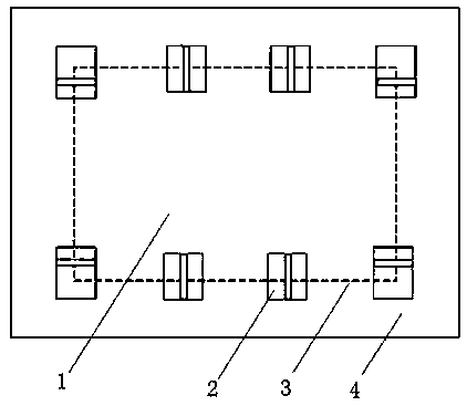
[0035] Such as Figure 1-7 For the embodiment of a kind of blind groove processing method of multilayer PCB board edge of the present invention, a kind of blind groove processing method of multilayer PCB board edge comprises the following steps:

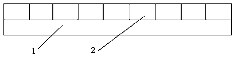
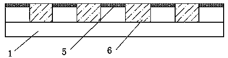
[0036] 1) Prepare a multi-layer PCB board 1 with a blind slot 4 structure;

[0037] 2) Prepare the protective film 5, and process the avoidance hole 51 on the protective film 5 corresponding to the position of the blind groo...


PUM


Abstract

The invention discloses a multilayered PCB edge blind slot processing method. The processing method comprises the following steps of 1) preparing a multilayered PCB with a blind slot structure; 2) preparing a protective film, and processing avoidance holes in the positions, corresponding to blind slots, in the protective film; 3) enabling the protective film and the blind slots to be aligned and pasted on the surface of the multilayered PCB, and then removing redundant air bubbles around the blind slots; 4) under the protection of the protective film, filling the blind slots by solidifiable filler; 5) after the solidifiable filler is solidified, removing the protective film from the surface; 6) performing milling and processing on the outline of the multilayered PCB, wherein the multilayered PCB is placed between two clamping elements in the milling and processing, and processing by a cutter to remove a to-be-cut part; and 7) removing the solidifiable filler from the blind slots. By adoption of the method, the blind slot structure with tidy edges and without burrs can be obtained, without requiring subsequent manual repair, so that the quality and the rate of finished products of the multilayered PCB with the board edge blind slot structure can be improved.

Description

technical field [0001] The invention relates to the field of mechanical processing, in particular to a method for processing blind grooves on the edge of a multilayer PCB board. Background technique [0002] The blind slot of a multi-layer PCB refers to a local area on the printed board that is formed by lamination, milling, etc. and has different heights. The main functions of the blind slot are as follows: one is to realize the input and output ports of the internal electrical signals of each layer; the other is to serve as a cavity and carrier for pasting and mounting chips, capacitors, resistors and other components; the third is to serve as a microwave component interconnection Connected channels are cascaded through gold wires, gold belts, etc. [0003] For the blind slots at the edge of the multilayer PCB, during the shape milling process, because these blind slots are in a "hollowed out" state, the material lacks support, and burrs are easily formed along the millin...

Claims


Application Information

Patent Timeline
Patent Type & Authority Patents(China)
IPC IPC(8): H05K3/46
CPCH05K3/46H05K2203/0228
Inventor 戴广乾刘军龚小林边方胜
Owner SOUTHWEST CHINA RES INST OF ELECTRONICS EQUIP
Why Eureka
Try Eureka