A fast thermal embossing process of polymer micro-nano structure differential temperature flat plate
A technology of micro-nano structure and flat plate hot pressing, which is applied in the field of polymer micro-nano structure differential temperature flat hot embossing process, which can solve the problems of serious time-consuming, demolding defects, prolonging the flat hot embossing process cycle, etc. The effects of small mold defects, low imprinting temperature, and shortened plate hot embossing cycle
- Summary
- Abstract
- Description
- Claims
- Application Information
AI Technical Summary
Problems solved by technology
Method used
Image
Examples
Embodiment 1
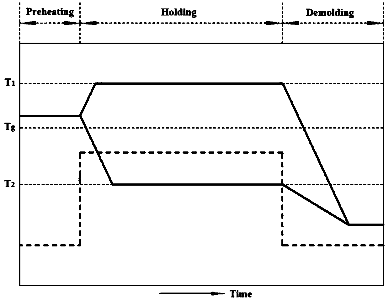
[0033] The present embodiment provides with 1mm thickness PMMA (T g =105°C) thin plate is the micro-nano structure thermal embossing method of substrate, the surface of the micro-nano structure mold used is a V-Cut structure with a characteristic size of 25 μm, comprising the following steps:
[0034] (1) Preheating: The PMMA substrate is preheated to 110°C, and the preheating process ensures that the temperature distribution of the polymer pressure surface is even;
[0035] (2) Embossing: The mold temperature on the side with V-Cut structure is set to 120°C, and the mold temperature on the side without structure is set to 100°C to ensure uniform temperature distribution on the mold surface. The material is embossed, the embossing pressure is set to 4Mpa, and the embossing time is set to 30s;
[0036] (3) Demoulding: After the thermal embossing micro-nano structure is filled, the mold temperature remains unchanged, and the mold is directly demoulded to obtain a polymer device...
Embodiment 2
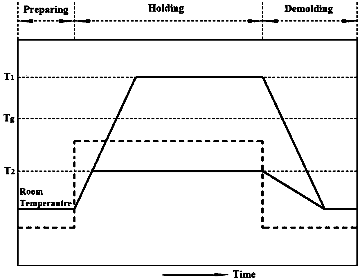
[0038] The present embodiment provides with 0.25mm thickness PC (T g =150°C) sheet is the micro-nano structure heat embossing method of base material, and the surface of the micro-nano structure mold used is a hemispherical structure with a diameter of 40 μm, comprising the following steps:
[0039] (1) Embossing: The temperature of the mold on the side with the hemispherical structure is set to 160°C, and the temperature of the mold on the side without the structure is set to 140°C to ensure uniform temperature distribution on the surface of the mold, and the mold directly performs thermal embossing on the PC substrate at room temperature , the embossing pressure is set to 8Mpa, and the embossing time is set to 60s;
[0040] (2) Demoulding: After the hot embossing is completed, the mold temperature is kept constant, and the mold is directly demoulded to obtain a polymer device with a hemispherical microstructure on the surface.
Embodiment 3
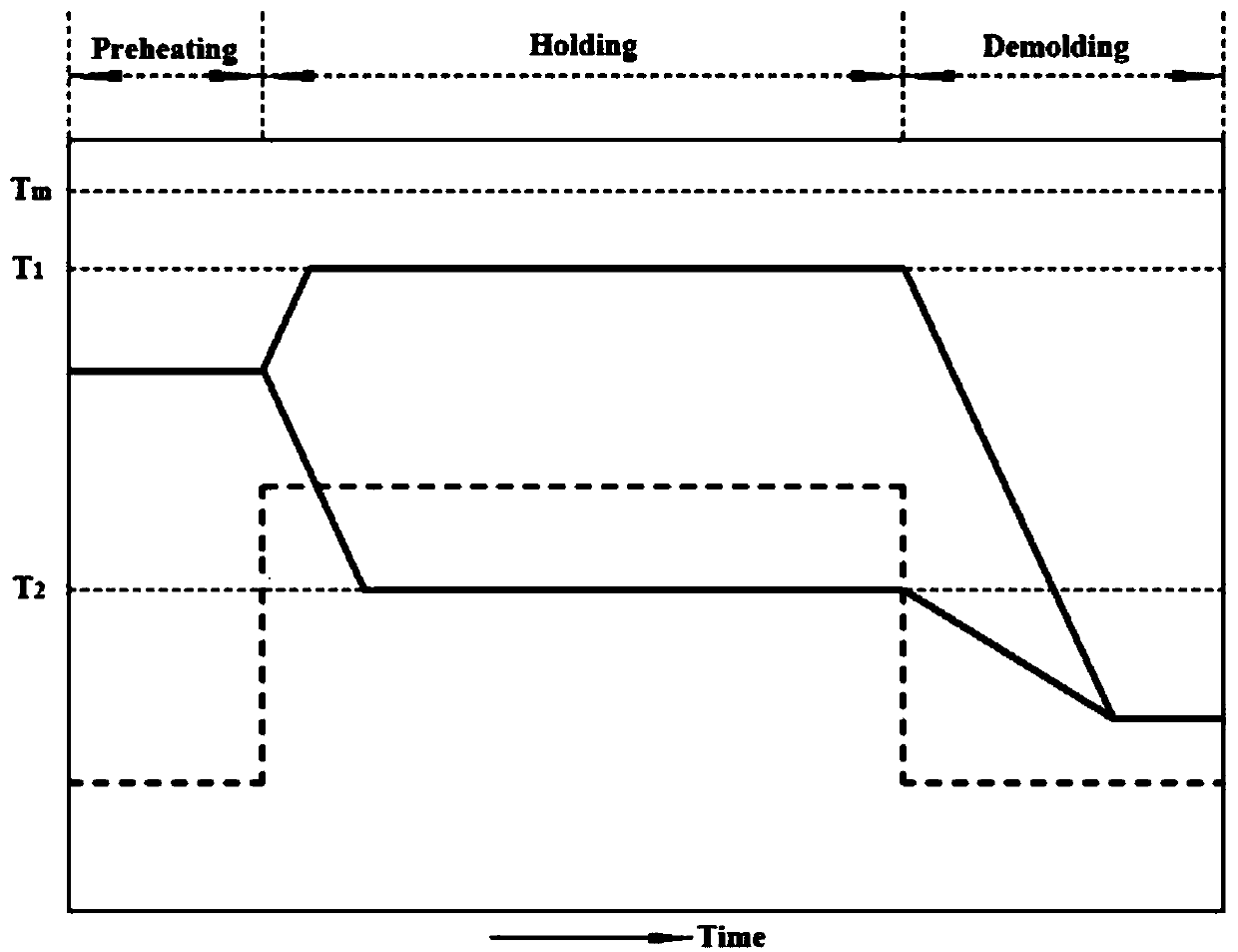
[0042] The present embodiment provides with 1mm thickness PMMA (T g =105 DEG C) thin plate is the micro-nano structure thermal embossing method of base material, and the micro-nano structure mold surface used is the nano cylinder structure that characteristic size is 200nm, comprises the following steps:
[0043] (1) Preheating: The PMMA substrate is preheated to 110°C, and the preheating process ensures that the temperature distribution of the polymer pressure surface is even;
[0044](2) Embossing: The temperature of the mold on the side with the nano-cylindrical structure is set to 125°C, and the mold temperature on the side without the structure is set to 95°C to ensure that the surface temperature of the mold is evenly distributed, and the mold is directly hot-pressed on the PMMA substrate at room temperature Printing, the printing pressure is set to 10Mpa, and the printing time is set to 90s;
[0045] (3) Demoulding: After the thermal embossing micro-nano structure is f...
PUM
| Property | Measurement | Unit |
|---|---|---|
| thickness | aaaaa | aaaaa |
| thickness | aaaaa | aaaaa |
| diameter | aaaaa | aaaaa |
Abstract
Description
Claims
Application Information


