An Array Layout Generation Method for Full Board Layout Resistor and Capacitance Extraction

A resistance-capacitance, layout technology, applied in electrical digital data processing, special data processing applications, instruments, etc., can solve the problem that the speed is difficult to meet the design requirements, the accurate calculation of the resistance and capacitance of the full board layout is time-consuming, and the array features no longer exist obviously, etc. question

Active Publication Date: 2020-06-16
北京华大九天科技股份有限公司
View PDF4 Cites 0 Cited by
  • Summary
  • Abstract
  • Description
  • Claims
  • Application Information

AI Technical Summary

Problems solved by technology

With the higher resolution and larger design size, especially the popularity of the In Cell process and the requirements for full board design, the accurate calculation of the full board layout resistors and capacitors is more time-consuming
The speed of traditional methods is difficult to meet the design requirements
[0003] In the full board design of touch screen and pixels, the hierarchical design method is usually adopted to make the touch screen unit and pixel unit into an array, but due to the access of other signal lines and the personal preference of the designer, the final layout hierarchy complex, array features no longer visibly present
Moreover, the graphics in the FPD layout are complex, and the precise extraction of resistors and capacitors is based on numerical analysis, and the speed is relatively slow.
Therefore, it is very time-consuming and even impossible to directly extract the resistors and capacitors of the full board layout.

Method used


Image

  • An Array Layout Generation Method for Full Board Layout Resistor and Capacitance Extraction
  • An Array Layout Generation Method for Full Board Layout Resistor and Capacitance Extraction
  • An Array Layout Generation Method for Full Board Layout Resistor and Capacitance Extraction

Examples


example

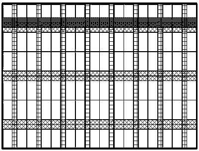
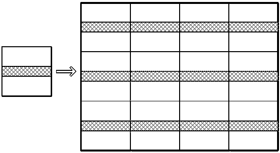
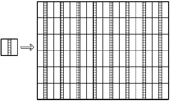
[0017] Combined with a specific example method, the operation process steps are as follows:

[0018] 1) Open a hierarchical layout;

[0019] 2) Select the reusable unit size w*h, and get the lower left corner of the array (x, y);

[0020] 3) Starting from (x, y), from left to right, from bottom to top, take an area of ​​size w*h, divide the layout, obtain candidate reusable graphics unit sequences, and perform each area Mark the corresponding serial number;

[0021] 4) Generate a new reusable array unit for each reusable graphics unit;

[0022] 5) Group the regions according to the region labels, and generate array instances according to the groups;

[0023] 6) A new layout is composed of new array instances.


PUM


Abstract

Due to the development of touch screen and pixel design technologies, the resolution is increasingly high, the size is increasingly large, and a more severe challenge is provided to the rate of extraction of the resistance capacitance from the full-panel layout. The extraction of the resistance capacitance from the full-panel layout by directly using the traditional numerical analysis method is too time-consuming. The extractive process can be accelerated by using a simple-structure multiplexing-array layout. However, difficulty is brought for array-based extraction methods due to unremarkable array features of an original layout. The invention provides a multiplexing-array layout generation method, and the original layout is decomposed into multiplexing-array-containing new layouts through multiplexing pattern element size selection, layout cutting, area grouping and new layout generation technologies by using repeated pattern features. Thus, an array structure of the full-panel layout is reconstructed, and the method is used for accelerating the extraction of the resistance capacitance from the full-panel layout.

Description

technical field [0001] The array layout generation method is a method for extracting the resistance and capacitance of the full board layout, and the invention belongs to the field of EDA design. Background technique [0002] The rapid development of flat panel display (FPD) process technology poses great challenges to design tools. The calculation of resistors and capacitors directly affects the overall performance of the FPD. Fast and accurate extraction of resistors and capacitors from large-scale layouts has become one of the key technologies in FPD design tools. With higher resolution and larger design size, especially the popularity of the In Cell process and the requirement for full board design, the accurate calculation of the resistors and capacitors of the full board layout is more time-consuming. The speed of the traditional method is difficult to meet the design requirements. [0003] In the full board design of touch screen and pixels, the hierarchical design...

Claims


Application Information

Patent Timeline
Patent Type & Authority Patents(China)
IPC IPC(8): G06F30/392
CPCG06F30/392
Inventor 贾艳明贾海涛陆涛涛
Owner 北京华大九天科技股份有限公司
Why Eureka
Try Eureka