chemical mechanical polishing device

A chemical machinery and polishing device technology, applied in grinding devices, grinding/polishing equipment, grinding machine tools, etc., can solve problems such as inability to accurately judge, and achieve the effect of improving accuracy

Active Publication Date: 2019-12-13
K C TECH
View PDF8 Cites 0 Cited by
  • Summary
  • Abstract
  • Description
  • Claims
  • Application Information

AI Technical Summary

Problems solved by technology

Therefore, among the output signals received by the thickness sensor 50 rotating together with the polishing pad 11 when it passes the lower side of the polishing head 20, it is impossible to accurately determine which part contains the thickness information of the polishing layer of the wafer W and which part contains the thickness information of the polishing layer of the wafer W. It is the part where the wafer W does not exist, which leads to the problem that the detection of the overall thickness distribution of the wafer can only be based on the deviation corresponding to the distance e1 and e2

Method used


Image

  • chemical mechanical polishing device
  • chemical mechanical polishing device
  • chemical mechanical polishing device

Examples


Embodiment Construction

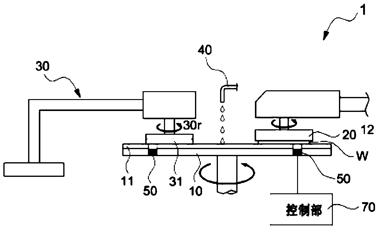
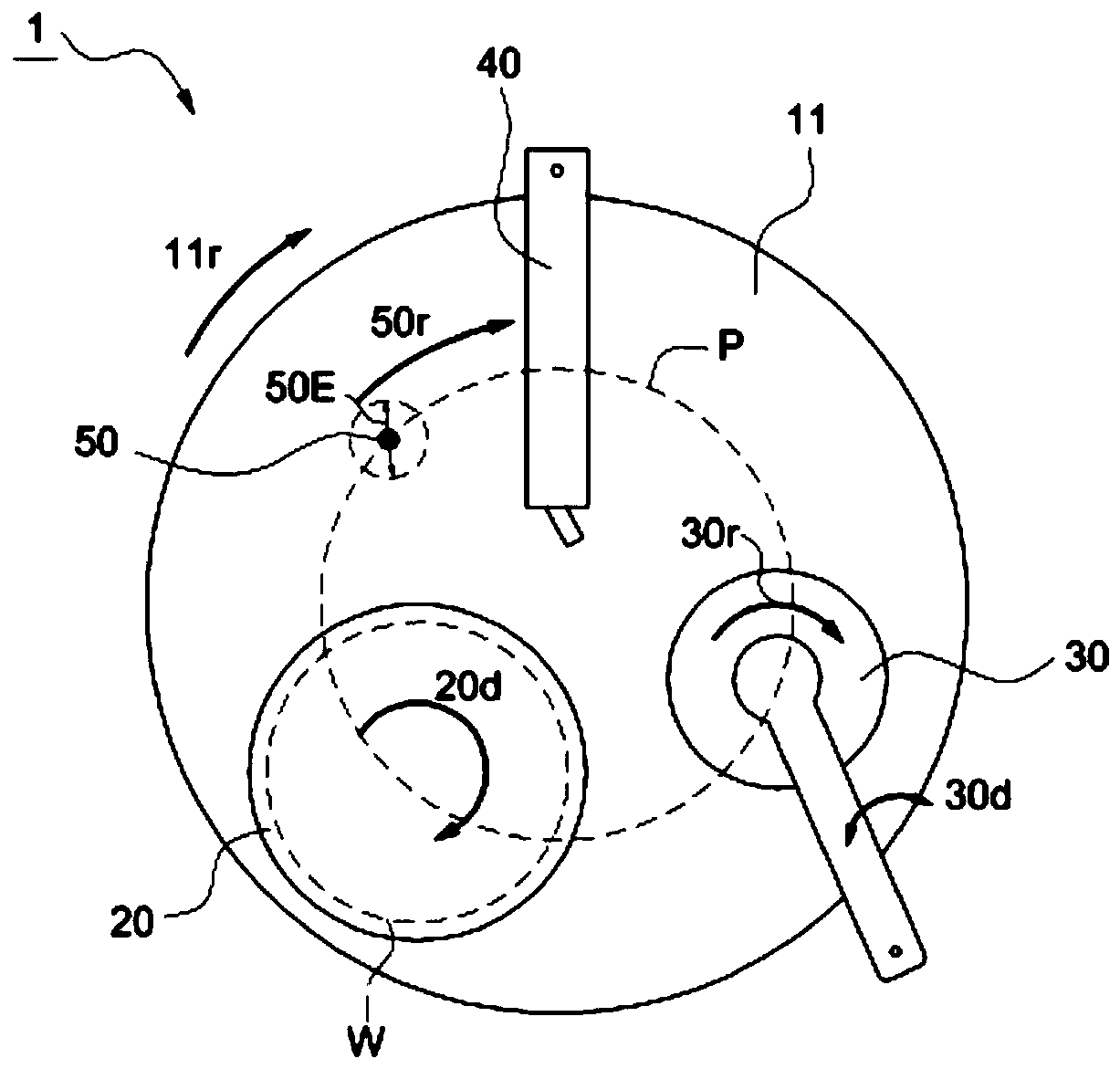
[0052] Next, a chemical mechanical polishing device 9 according to an embodiment of the present invention will be described in detail with reference to the drawings. However, in describing the present invention, detailed descriptions of well-known functions and configurations will be omitted in order to clarify the gist of the present invention.

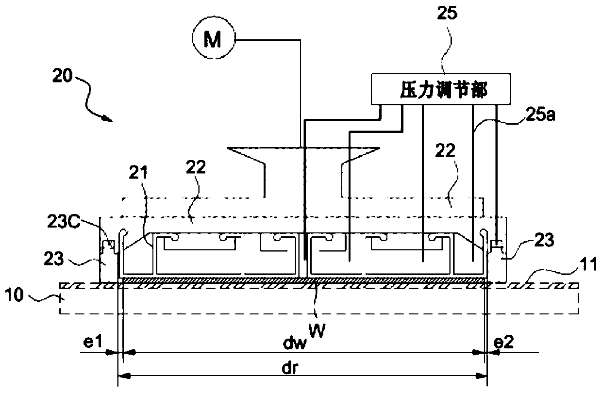
[0053] A chemical mechanical polishing device 9 related to an embodiment of the present invention includes: a polishing flat plate 10 covered with a polishing pad 11, and the above-mentioned polishing pad 11 is in contact with the polishing layer of the wafer W formed with a conductive polishing layer to achieve polishing; The head 100 pressurizes the wafer W while it is on the bottom surface and rotates the wafer W; the thickness sensor 50 applies an eddy current to detect the thickness of the polishing layer of the wafer W and receives an output signal from the polishing layer; and the control unit 90 An AC current is applied to th...


PUM

PropertyMeasurementUnit
thicknessaaaaaaaaaa

Abstract

The present invention relates to a chemical mechanical polishing apparatus. The chemical mechanical polishing apparatus includes: an abrasive platen which has an abrasive pad applied on the upper surface and rotates; an abrasive head having a retainer ring including a first member which is made of a conductive material and is formed on a wafer and a second member which is made of a non-conductive material and is formed on the lower part of the first member to come in contact with the abrasive pad during a chemical mechanical polishing process while coming in contact with the platen surface of the wafer during the chemical mechanical polishing process to press the plate surface; a thickness sensor which is fixed on the abrasive platen, rotates with the abrasive pad, applies an eddy current signal to the wafer, and receives an output signal including the thickness information of the wafer polishing layer; and a control unit which obtains the thickness of the wafer polishing layer in the polishing layer area occupied by the wafer polishing layer from a reference location being the location of the first member from the thickness sensor. The thickness sensor rapidly changes the magnitude of an output voltage of the output signal received thereto as passing through the first member, thereby sensing the location of the wafer polishing layer by using the changed location of the output voltage as the reference location.

Description

technical field [0001] The present invention relates to a chemical mechanical polishing device, and more particularly to a chemical mechanical polishing device for accurately identifying the polishing layer thickness distribution of a wafer by accurately detecting the position of the polishing layer as an object to be polished in a chemical mechanical polishing process. Background technique [0002] In general, chemical mechanical polishing (CMP) is a process in which a substrate such as a wafer is in contact with the polishing plate on a rotating polishing plate to perform mechanical polishing by rotating it, This makes the surface of the substrate flattened to a predetermined thickness. [0003] For this, as figure 1 As shown, in the chemical mechanical polishing apparatus 1, the polishing plate 12 is rotated with the upper part covered with the polishing pad 11, and the wafer W is pressed against the surface of the polishing pad 11 by using the polishing head 20 and rota...

Claims


Application Information

Patent Timeline
Patent Type & Authority Patents(China)
IPC IPC(8): B24B37/013B24B37/10B24B37/32B24B49/04B24B49/10
CPCB24B37/013B24B37/10B24B37/32B24B49/04B24B49/105
Inventor 金钟千金旻成赵玟技
Owner K C TECH
Why Eureka
Try Eureka