Touch display screen
A touch display and LCD technology, applied in the display field, can solve the problems of poor user experience, multiple reflections, poor display effect, etc., and achieve the effect of improving anti-interference ability, high surface hardness and large screen size
- Summary
- Abstract
- Description
- Claims
- Application Information
AI Technical Summary
Problems solved by technology
Method used
Image
Examples
Embodiment 1
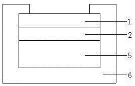
[0014] Such as figure 1 As shown, the touch display screen includes a first thin film sensor layer 1, a liquid crystal screen 5 and a housing 6; the first thin film sensor layer 1 is bonded together with the liquid crystal screen 5 through the first OCA optical adhesive layer 2; the second A film sensor layer 1 and a liquid crystal screen 5 are installed inside the casing 6 , and the casing 6 is provided with flanges around the periphery, and the flanges are pressed against the outer surface of the first film sensor layer 1 .
[0015] When the first thin film sensor layer 1 is touched, an electronic signal will be sent back to the inside of the IC to realize the touch effect.
[0016] The first OCA optical adhesive layer 2 is used for bonding, which has good transparency, mature technology, and good bonding effect. There is no air layer, and the reflection is reduced by 8%, which improves the display effect.
[0017] The size of the capacitance is related to the conductive ar...
Embodiment 2
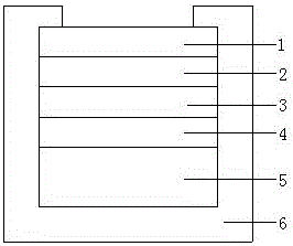
[0022] Such as figure 2 As shown, the touch display screen includes a first film sensor layer 1, a second film sensor layer 3, a liquid crystal screen 5 and a housing 6; the first film sensor layer 1 passes through the first OCA optical adhesive layer 2 and the second film sensor layer 3 Paste together, the second thin film sensor layer 3 is pasted together with the liquid crystal screen 5 through the second OCA optical glue layer 4, and the first thin film sensor layer 1, the second thin film sensor layer 3 and the liquid crystal screen 5 are installed on the shell 6 Inside, the shell 6 is provided with flanging around the periphery, and the flanging is pressed against the surface of the first film sensor layer 1 .
[0023] The first thin film sensor layer 1 and the second thin film sensor layer 3 are respectively coated with different shapes as capacitive sensing electrodes with conductive coatings, so that when a finger touches, the capacitive sensing value can be changed ...
PUM
 Abstract
Description
Claims
Application Information

