Rectifier bridge structure for on-chip integration

A rectifier bridge and minority carrier technology, applied in the field of circuits, can solve the problems of parasitic leakage of the rectifier bridge, which is not conducive to improving product integration, product miniaturization, and intelligent development, and achieves the effect of improving integration.

Active Publication Date: 2017-06-13
南京国博电子股份有限公司
View PDF8 Cites 2 Cited by
  • Summary
  • Abstract
  • Description
  • Claims
  • Application Information

AI Technical Summary

Problems solved by technology

[0003] In most cases of modern chip manufacturing, P-type materials are used as the substrate of the wafer. When designing the chip, the GND pin of the chip is also connected to the P-type substrate of the wafer. Due to the diode production process, each diode’s There will be parasitic transistors in the structure. When the main chip circuit and the rectifier bridge are set on the same substrate, the voltage of the GND pin of the chip connected to the P-type substrate will no longer be the lowest voltage of the whole circuit, resulting in parasitic leakage of the rectifier bridge.
[0004] Therefore, most of the systems that use AC power and non-polar voltage power supply use off-chip rectifier bridges, which is not conducive to improving product integration and the development of product miniaturization and intelligence.

Method used


Image

  • Rectifier bridge structure for on-chip integration
  • Rectifier bridge structure for on-chip integration
  • Rectifier bridge structure for on-chip integration

Examples


Embodiment Construction

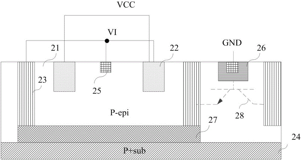
[0018] In order to make the object, technical solution and advantages of the present invention clearer, the implementation manner of the present invention will be further described in detail below in conjunction with the accompanying drawings.

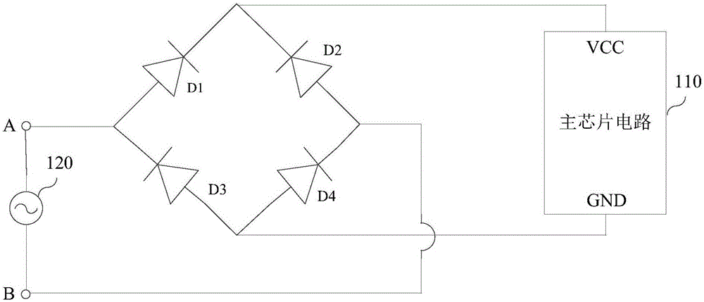
[0019] figure 1 A schematic circuit diagram of a rectifier bridge is shown. Diodes D1 , D2 , D3 , D4 form a rectifier bridge, and the rectifier bridge is connected with the main chip circuit 110 and the power supply 120 . Optionally, the power supply 120 is an AC power supply or a non-polar power supply.

[0020] The rectifier bridge is connected to the VCC terminal and the GND terminal of the main chip circuit 110 .

[0021] Assuming that the high voltage of the power supply 120 is Vh, and the low voltage is Vl, when the A terminal is at the high voltage Vh, and the B terminal is at the low voltage Vl, the diodes D1 and D4 are turned on at the same time, and when the A terminal is at the low voltage V1, and the B terminal is at the ...


PUM


Abstract

The invention discloses a rectifier bridge structure for on-chip integration and belongs to the circuit field. The rectifier bridge structure comprises four diodes and two minority carrier guard rings that constitute the rectifier bridge. Each of the first and second diodes in the four diodes is surrounded by a minority carrier guard ring. Each minority carrier guard ring is composed of a deep N-well (DNW) and a buried N layer (BN) located below the DNW and passes through the P-type epitaxial layer where the corresponding diode is located. The DNW in the minority carrier guard ring is connected with a P-type source-drain (PSD) via a metallic wire. The PSD is surrounded by a shallow P-well (SPWELL). The rectifier bridge structure solves a problem that parasitic leakage occurs when the rectifier bridge and a main chip are integrated into the same substrate in the prior art. Thus, the rectifier bridge and the main chip can be integrated into the same substrate and a product integration level is improved.

Description

technical field [0001] The embodiments of the present invention relate to the field of circuits, in particular to a rectifier bridge structure for on-chip integration. Background technique [0002] A rectifier bridge is used to convert AC voltage or non-polar voltage into DC voltage. Most of the systems powered by AC voltage or non-polar power supply are provided with a rectifier bridge. [0003] In most cases of modern chip manufacturing, P-type materials are used as the substrate of the wafer. When designing the chip, the GND pin of the chip is also connected to the P-type substrate of the wafer. Due to the diode production process, each diode’s There will be parasitic transistors in the structure. When the main chip circuit and the rectifier bridge are set on the same substrate, the voltage of the GND pin of the chip connected to the P-type substrate will no longer be the lowest voltage of the whole circuit, resulting in parasitic leakage of the rectifier bridge. . [...

Claims


Application Information

Patent Timeline
Patent Type & Authority Applications(China)
IPC IPC(8): H01L27/04H02M7/06
CPCH01L27/04H02M7/06
Inventor 徐义强康明辉范建林朱波曾红霞
Owner 南京国博电子股份有限公司
Why Eureka
Try Eureka