
Method for determining PCB (printed circuit board) inner layer film compensation coefficient

A technology of compensation coefficient and inner layer, applied in multilayer circuit manufacturing, electrical components, printed circuit manufacturing, etc., can solve problems such as out-of-synchronization of core board thermal stress release, lower alignment between layers, inconsistent expansion and contraction, etc., to achieve Low cost, improved alignment between layers, and improved product quality

Active Publication Date: 2017-06-13
奥士康精密电路(惠州)有限公司
View PDF4 Cites 6 Cited by
  • Summary
  • Abstract
  • Description
  • Claims
  • Application Information

AI Technical Summary

Problems solved by technology

In the PCB industry, it is easier to establish the film coefficient of the inner layer of the board with the same thickness of the inner core board of the multi-layer board, but when the thickness of the core board is inconsistent, due to the asynchronous release of thermal stress of the core boards of different thicknesses, the expansion and contraction of the board will occur when the board is pressed. Inconsistency leads to riveting deviation, thereby reducing the alignment between layers, and it is easy to drill deviation and cause internal short scrapping

Method used


Image

  • Method for determining PCB (printed circuit board) inner layer film compensation coefficient

Examples


Embodiment Construction

[0020] The present invention will be further described below in conjunction with the accompanying drawings and specific embodiments.

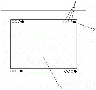
[0021] figure 1 The reference numbers in the figure are: inner layer film 1; solid measurement target 2; hollow measurement target 3.

[0022] This embodiment is applied to a six-layer PCB board, and provides a method for determining the film compensation coefficient of the PCB inner layer, including the following steps:

[0023] (1) For the design of the inner layer film 1, a total of four sets of measurement targets are set along the edge of the board on the corresponding inner layer film of each inner layer of the PCB in the four corner areas; the number of inner layers of the PCB is 4. Each layer of the inner layer can be defined as the nth layer according to the positional relationship from top to bottom; figure 1 As shown, each group of measurement marks set on the fifth layer of the PCB, that is, the inner film 1 corresponding to the f...


PUM


Abstract

The invention provides a method for determining the PCB (printed circuit board) inner layer film compensation coefficient. The method comprises the following steps of (1) designing an inner layer film; (2) performing primary measurement on an expansion and shrinkage value in a measuring mode of performing quadratic element measurement on each layer of board of an etched PCB and then calculating the expansion and shrinkage extreme difference; (3) performing secondary measurement on the expansion and shrinkage value in a measuring mode of performing X-RAY measurement on each layer of board of the PCB subjected to board pressing and then calculating the expansion and shrinkage extreme difference; (4) determining the compensation coefficient of each inner layer film according to the obtained expansion and shrinkage extreme difference. The method has the advantages that the inner layer film compensation coefficient is obtained through comparing different expansion and shrinkage data; the PCB lamination expansion and shrinkage can be controlled; the influence on the PCB alignment precision is reduced; the method is practical; the operation is easy; the cost is low; the rejection rate of the multilayer board can be effectively reduced.

Description

technical field [0001] The invention relates to the field of PCB, in particular to a method for determining the film compensation coefficient of the inner layer of the PCB. Background technique [0002] With the development of the electronics industry, PCB design is increasingly developing towards high-level, dense lines, and small-pitch BGA, which puts forward high alignment accuracy requirements for PCB manufacturers. Usually the biggest factor affecting PCB alignment accuracy is expansion and contraction, so how to analyze and control the expansion and contraction of PCB lamination becomes extremely critical. In the PCB industry, it is easier to establish the film coefficient of the inner layer of the board with the same thickness of the inner core board of the multi-layer board, but when the thickness of the core board is inconsistent, due to the asynchronous release of thermal stress of the core boards of different thicknesses, the expansion and contraction of the board...

Claims


Application Information

Patent Timeline
Patent Type & Authority Applications(China)
IPC IPC(8): H05K3/46
CPCH05K3/4638H05K2203/166
Inventor 叶志诚黄勇贺波
Owner 奥士康精密电路(惠州)有限公司
Learn More