A kind of manufacturing method of hdi board

A manufacturing method and sub-board technology, which are applied in multilayer circuit manufacturing, printed circuit manufacturing, electrical components, etc., can solve the problems that PIN holes cannot meet the manufacturing requirements, and the processing technology of PIN holes needs to be improved, so as to improve product yield, The effect of improving design ability and improving inter-layer alignment

Active Publication Date: 2020-12-08
DONGGUAN SHENGYI ELECTRONICS
View PDF8 Cites 0 Cited by
  • Summary
  • Abstract
  • Description
  • Claims
  • Application Information

AI Technical Summary

Problems solved by technology

However, when the thickness of the sub-board is large, the PIN holes formed by stamping often cannot meet the production requirements, so the processing technology of the PIN holes needs to be improved.

Method used


Image

  • A kind of manufacturing method of hdi board
  • A kind of manufacturing method of hdi board
  • A kind of manufacturing method of hdi board

Examples


Embodiment Construction

[0043] In order to make the purpose, features and advantages of the present invention more obvious and understandable, the technical solutions in the embodiments of the present invention will be clearly and completely described below in conjunction with the accompanying drawings in the embodiments of the present invention. Obviously, the following The described embodiments are only some, not all, embodiments of the present invention. Based on the embodiments of the present invention, all other embodiments obtained by persons of ordinary skill in the art without making creative efforts belong to the protection scope of the present invention.

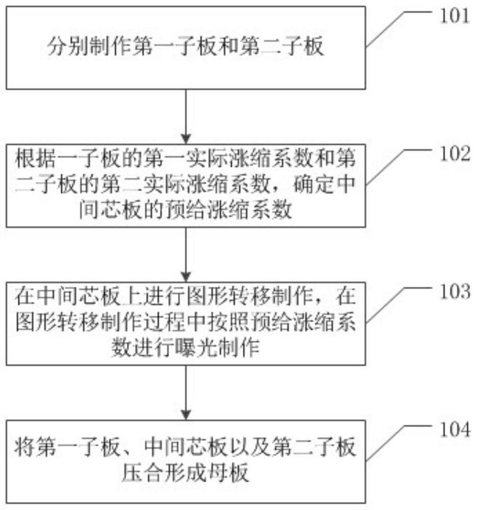
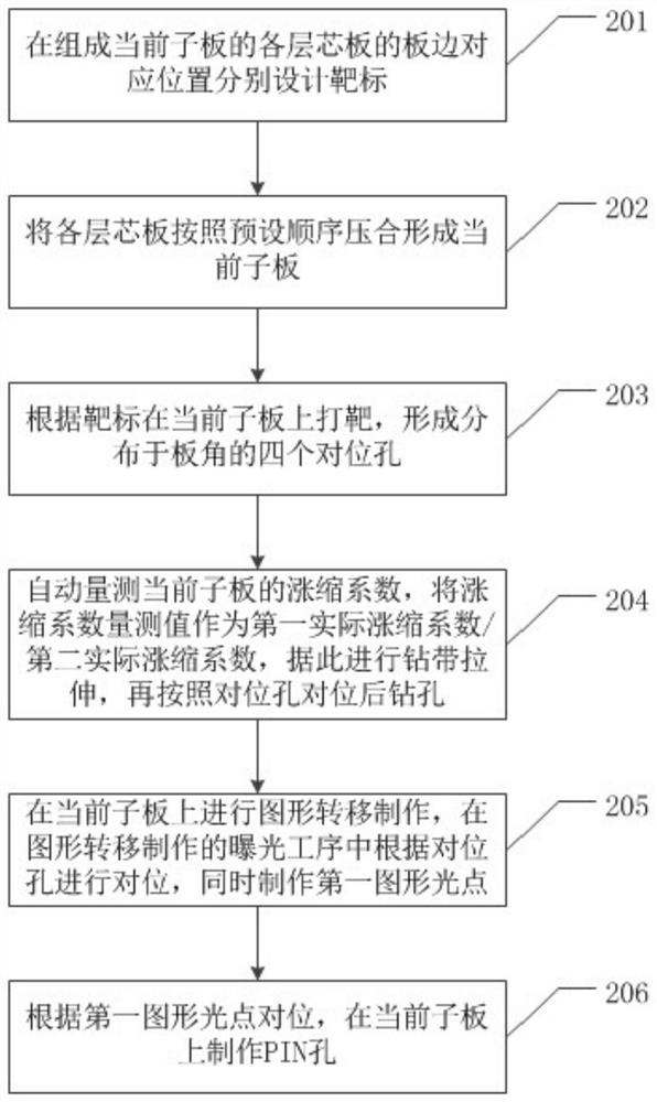
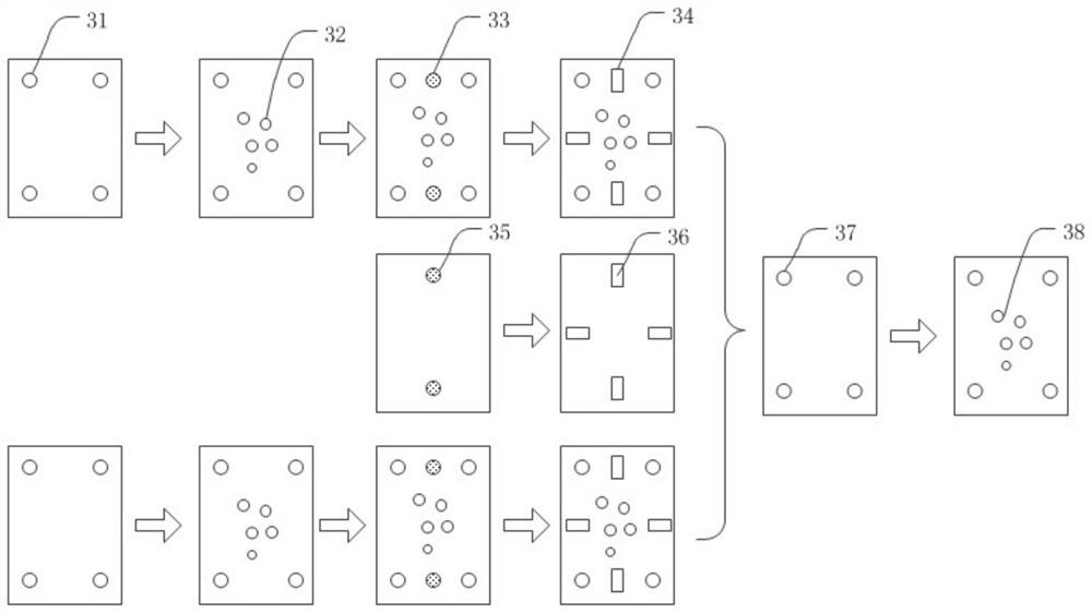
[0044] see figure 1 , an embodiment of the present invention provides a method for manufacturing an HDI board. The HDI board is made by laminating a first sub-board, at least one intermediate core board, and a second sub-board. The manufacturing method specifically includes:

[0045] Step 101, making a first sub-board and a second sub-bo...


PUM


Abstract

The invention relates to the technical field of PCBs, and discloses a PIN hole processing method and a manufacturing method of an HDI board. The PIN hole machining method comprises the steps of drilling holes at the two ends, in the length direction, of a designated setting area respectively, and forming two guide holes with the diameter smaller than a preset PIN hole width; performing reaming operation on the two guide holes to form two reamed holes of which the diameters are equal to the preset PIN hole width; and performing at least one time of supplementary drilling operation between the two reamed holes until the PIN hole is formed. The manufacturing method of the HDI board comprises the following steps of respectively manufacturing a first daughter board and a second daughter board;according to the actual expansion and shrinkage coefficients of the two daughter boards, determining a preset expansion and shrinkage coefficient of a middle core board; carrying out exposure manufacturing on the middle core plate according to a preset expansion and shrinkage coefficient; and laminating the first daughter board, the middle core board and the second daughter board to form a motherboard. According to the embodiment of the invention, the interlayer alignment degree of the HDI board can be effectively improved, the PIN hole processing precision also can be effectively improved, and the method is especially suitable for the daughter boards with larger board thicknesses.

Description

technical field [0001] The invention relates to the technical field of PCB (Printed Circuit Board, printed circuit board), in particular to a method for manufacturing an HDI board. Background technique [0002] With the development of PCB to high-layer boards, the alignment requirements are getting higher and higher, and the manufacturing difficulty is getting more and more difficult. This is due to the fact that there are many factors that affect the alignment capability, involving multiple processes in the entire PCB manufacturing process. Poor alignment will lead to PCB short circuit, poor signal, CAF and other undesirable phenomena. Therefore, improving the alignment capability plays a key role in improving the PCB process capability and enhancing the market competitiveness of enterprises. [0003] For N+2+…+2+N type mechanical HDI boards (also known as S boards), there is no clear alignment control specification at present, and the expansion and contraction coefficient...

Claims


Application Information

Patent Timeline
Patent Type & Authority Patents(China)
IPC IPC(8): H05K3/46H05K3/00
CPCH05K3/0047H05K3/4611
Inventor 宋清唐海波刘梦茹纪成光陈正清
Owner DONGGUAN SHENGYI ELECTRONICS
Why Eureka
Try Eureka