Pixel circuit and driving method thereof and organic light emitting display
A pixel circuit and organic technology, applied in the field of organic light-emitting displays, can solve problems such as image sticking, and achieve the effect of avoiding threshold voltage deviation and threshold voltage drift.
- Summary
- Abstract
- Description
- Claims
- Application Information
AI Technical Summary
Problems solved by technology
Method used
Image
Examples
Embodiment 1
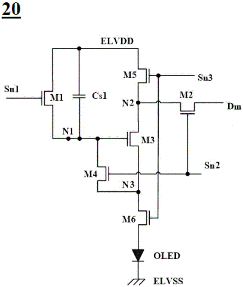
[0036] Please refer to figure 2 , which is a schematic structural diagram of a pixel circuit according to Embodiment 1 of the present invention. The pixel circuit 20 includes:
[0037] The first transistor M1 is connected between the first power supply ELVDD and the first node N1, and its gate is connected to the first scan line Sn1;
[0038] The second transistor M2 is connected between the data line Dm and the second node N2, and its gate is connected to the second scan line Sn2;
[0039] The third transistor M3 is connected between the second node N2 and the third node N3, and its gate is connected to the first node N1;
[0040] The fourth transistor M4 is connected between the first node N1 and the third node N3, and its gate is connected to the second scan line Sn2;
[0041] The fifth transistor M5 is connected between the first power supply ELVDD and the second node N2, and its gate is connected to the third scan line Sn3;
[0042] The sixth transistor M6 is connect...
Embodiment 2
[0076] Please refer to Figure 4 , which is a schematic structural diagram of a pixel circuit according to Embodiment 2 of the present invention. The pixel circuit 30 includes:
[0077] The first transistor M1 is connected between the first power supply ELVDD and the first node N1, and its gate is connected to the first scan line Sn1;
[0078] The second transistor M2 is connected between the data line Dm and the second node N2, and its gate is connected to the second scan line Sn2;
[0079] The third transistor M3 is connected between the second node N2 and the third node N3, and its gate is connected to the first node N1;
[0080] The fourth transistor M4 is connected between the first node N1 and the third node N3, and its gate is connected to the second scan line Sn2;
[0081] The fifth transistor M5 is connected between the first power supply ELVDD and the second node N2, and its gate is connected to the third scan line Sn3;
[0082] The sixth transistor M6 is connect...
PUM
 Abstract
Description
Claims
Application Information


