Display device, array substrate and pixel unit

A technology for pixel units and array substrates, applied in electrical components, optics, instruments, etc., can solve problems such as increased power consumption, inability to achieve various brightness and different power consumption requirements, and adverse adjustment, and achieve the effect of meeting user needs.

Inactive Publication Date: 2017-07-07
BOE TECH GRP CO LTD +1
View PDF10 Cites 0 Cited by
  • Summary
  • Abstract
  • Description
  • Claims
  • Application Information

AI Technical Summary

Problems solved by technology

[0003] In the prior art, the structure and working mode of the existing pixel unit are single, in order to obtain high transmittance and high brightness to improve the display effect, the driving voltage will be increased, and the power consumption will be increased accordingly; Reducing power consumption will reduce the transmittance and brightness, and can only display the display effect of low gray scale and low brightness images; therefore, it is impossible to achieve multiple brightness and different power consumption requirements, and the scope of application is small. It is convenient for users to adjust according to the actual situation

Method used


Image

  • Display device, array substrate and pixel unit
  • Display device, array substrate and pixel unit
  • Display device, array substrate and pixel unit

Examples


Embodiment approach

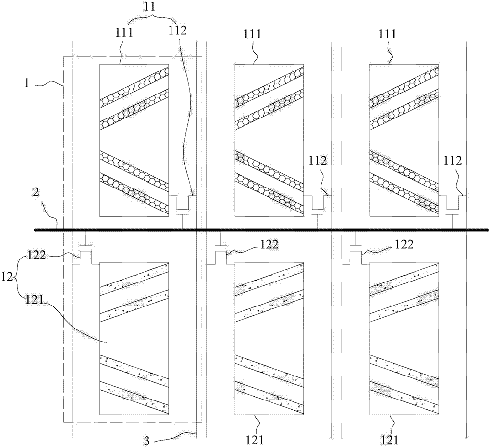
[0072] Example embodiments of the present disclosure provide an array substrate, such as Image 6 , the array substrate in this embodiment may include gate lines 2 , data lines 3 and pixel units.

[0073] In this embodiment, the composition of the pixel unit can refer to the pixel unit in the above embodiment of the pixel unit; Image 6For the arrangement of the gate lines 2 and the data lines 3, reference may be made to the related content in the first embodiment of the above array substrate, which will not be repeated here; in addition, each first sub-sub-pixel 11 and each second sub-sub-pixel 12 are It can be divided into two rows, and the first sub-sub-pixel 11 and the second sub-sub-pixel 12 are distributed in any row, and the first sub-sub-pixel 11 and the second sub-sub-pixel 12 in each row are arranged at intervals.

[0074] The above-mentioned array substrates of the first embodiment and the second embodiment can simultaneously send signals to the first thin film tra...


PUM


Abstract

The invention provides a display device, an array substrate and a pixel unit. The pixel unit comprises a plurality of subpixels, wherein each sub-pixels comprises a first child subpixel and a second child subpixel; the first child subpixel comprises a first pixel electrode and a first thin-film transistor; the first pixel electrode is provided with a plurality of slits with a first width and a plurality of first sub-electrodes partitioned by the slits; a control end of the first thin-film transistor is connected to a first gate line, a first end is connected to a first data line and a second end is connected to the first pixel electrode; the second child subpixel comprises a second pixel electrode and a second thin-film transistor; the second pixel electrode comprises a plurality of slits with a second width and a plurality of second sub-electrodes partitioned by the slits, and the second width is not equal to the first width; and the control end of the second thin-film transistor is connected to a second gate line, the first end is connected to a second data line and the second end is connected to the second pixel electrode.

Description

technical field [0001] The present disclosure relates to the field of display technology, and in particular, to a display device, an array substrate and a pixel unit. Background technique [0002] Currently, in the field of thin film transistor liquid crystal displays, IPS (In-Plane Field Effect) displays and FFS (Fringe Field Effect) displays are widely used because of their advantages of wide viewing angle, high transmittance, and fast response. For the existing IPS display and FFS display, the array substrates of both include a plurality of pixel units distributed in an array, and each pixel unit includes a plurality of sub-pixels; the pixel electrodes of these sub-pixels generally adopt upper and lower dual-domain Symmetrical slit electrodes. Among them, the electrode spacing of the slit electrodes has a relatively obvious influence on the display effect. In other words, the smaller the electrode spacing, the higher the transmittance and driving voltage of liquid cryst...

Claims


Application Information

Patent Timeline
Patent Type & Authority Applications(China)
IPC IPC(8): G02F1/1343G02F1/1362H01L27/12
CPCG02F1/134309G02F1/134363G02F1/136286G02F1/134345G02F1/134372H01L27/1214
Inventor 干泉王永灿马睿
Owner BOE TECH GRP CO LTD
Why Eureka
Try Eureka