Wafer defect detection method

A detection method and defect technology, applied in the direction of semiconductor/solid-state device testing/measurement, electrical components, circuits, etc., can solve problems such as detection equipment scanning termination, achieve the effect of reducing hardware configuration requirements, improving product yield, and being easy to implement

Active Publication Date: 2017-07-21
SHANGHAI HUALI MICROELECTRONICS CORP
View PDF3 Cites 24 Cited by
  • Summary
  • Abstract
  • Description
  • Claims
  • Application Information

AI Technical Summary

Problems solved by technology

[0005] The purpose of the present invention is to provide a detection method for wafer defects, to solve the problem of filtering out defects other than chromatic aberration defects to a large extent in the prior art, and some detection areas have too many defects, resulting in detection Device scan terminated issue

Method used


Image

  • Wafer defect detection method
  • Wafer defect detection method
  • Wafer defect detection method

Examples


Embodiment Construction

[0050] The specific implementation manner of the present invention will be described in more detail below with reference to schematic diagrams. Advantages and features of the present invention will be apparent from the following description and claims. It should be noted that all the drawings are in a very simplified form and use imprecise scales, and are only used to facilitate and clearly assist the purpose of illustrating the embodiments of the present invention.

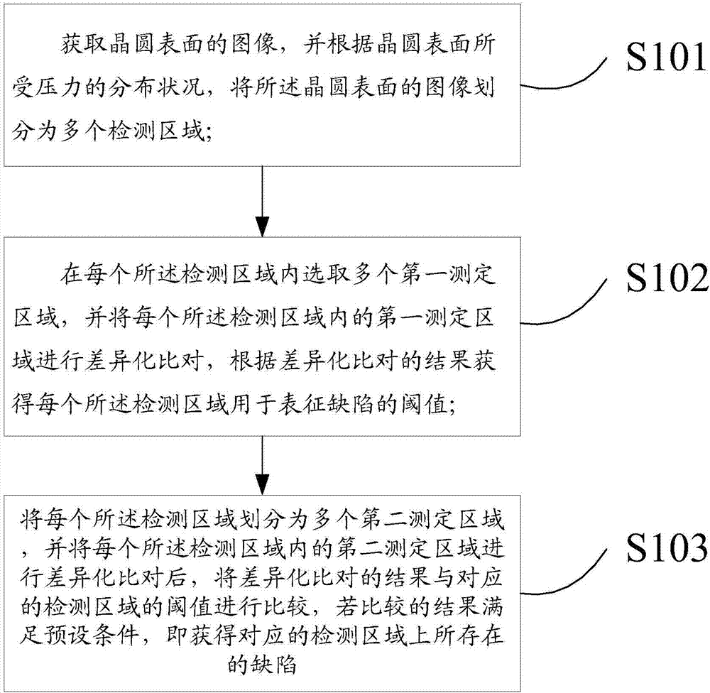
[0051] figure 2 The flowchart of the method for detecting wafer defects provided by the embodiment of the present invention, such as figure 2 As shown, the wafer defect detection method includes step S101, step S102 and step S103.

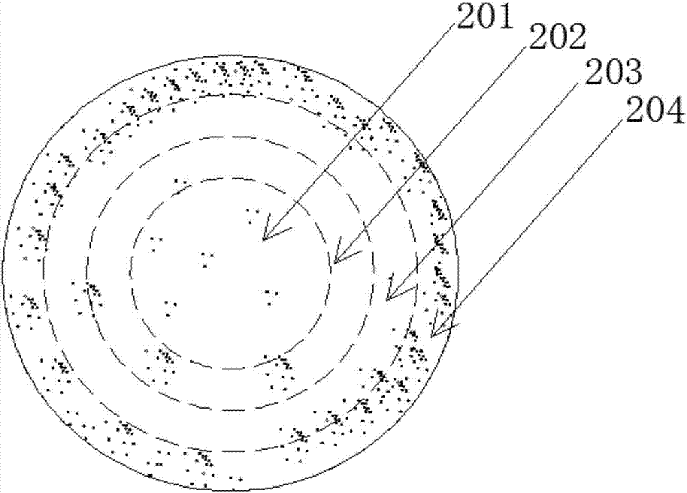
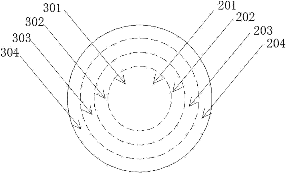
[0052] Wherein, step S101: acquire an image of the wafer surface, and divide the image of the wafer surface into a plurality of detection areas according to the distribution of pressure on the wafer surface.

[0053] Specifically, due to the Poly CMP (Polysilicon Floating Gate Ch...


PUM


Abstract

The invention provides a wafer defect detection method comprising the steps that the image of the surface of a wafer is acquired, and the image of the surface of the wafer is divided into multiple detection areas; multiple first determination areas are selected in each detection area, differential comparison is performed on the first determination areas in each detection area, and the threshold of each detection area for representing the defect is acquired according to the result of differential comparison; and each detection area is divided into multiple second determination areas and differential comparison is performed on the second determination areas in each detection area and then the result of differential comparison is compared with the threshold of the corresponding detection area, and the defect existing in the corresponding detection area can be acquired if the result of comparison meets the preset conditions. Different thresholds are set for different detection areas to obtain the corresponding defect number of different detection areas so that more polysilicon residual defects can be captured and the detection accuracy can be enhanced.

Description

technical field [0001] The invention relates to the field of semiconductor manufacturing, in particular to a method for detecting wafer defects. Background technique [0002] In the field of semiconductor manufacturing, after the wafer is chemically mechanically polished, it is necessary to scan and determine the number of defects on the wafer to achieve the purpose of checking whether the process meets the requirements. [0003] In actual production, the polishing head of the chemical mechanical polishing machine can optimize the flatness of the wafer by controlling different pressures on different regions of the wafer. During the process of grinding the wafer, the grinding head presses down on the wafer and the grinding table moves relative to each other. Because the pressure of the grinding head on different areas of the wafer is different, it is easy to cause large differences in the grinding thickness of some areas of the wafer. There are other areas where the differen...

Claims


Application Information

Patent Timeline
Patent Type & Authority Applications(China)
IPC IPC(8): H01L21/66
CPCH01L22/12
Inventor 郭贤权许向辉陈昊瑜
Owner SHANGHAI HUALI MICROELECTRONICS CORP
Why Eureka
Try Eureka