Testing method for CMOS sensors

A technology of CMOS sensor and test method, which is applied in the direction of TV, electrical components, image communication, etc., can solve the problems of small number of tests, few test functions, single performance of CMOS sensor circuit and pixel, etc., so as to improve test convenience and increase functions Sexuality and cost reduction effect

Active Publication Date: 2017-07-28
国芯微(重庆)科技有限公司
View PDF8 Cites 2 Cited by
  • Summary
  • Abstract
  • Description
  • Claims
  • Application Information

AI Technical Summary

Problems solved by technology

[0003] Existing test systems usually can only test the circuit and pixel performance of CMOS sensors, and can only test one CMOS sensor chip
It has the technical problems of few test functions and a small number of tests

Method used


Image

  • Testing method for CMOS sensors
  • Testing method for CMOS sensors
  • Testing method for CMOS sensors

Examples


Embodiment 1

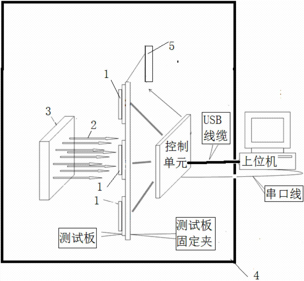
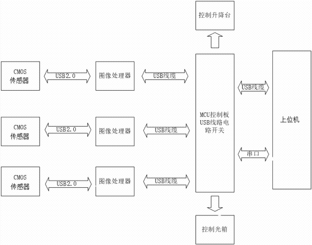
[0061] This embodiment provides a test system for CMOS sensors, such as figure 1 , the test system includes a parallel light light box that provides parallel light, the parallel light light box is a DNP light box; the number is 3 lensless CMOS sensors, and the lensless CMOS sensor corresponds to the position of the parallel light during testing; Describe the test board that no lens CMOS sensor is connected, described test board includes the image sensor that is used to collect signal data; Described no lens CMOS sensor and test board are all fixed on test board holder, and described test board holder is fixedly connected to Lifting platform; the test board is connected to the control unit through USB2.0, the control unit is also connected to the lifting platform, and the control unit is connected to the upper computer through a USB cable and serial port; the upper computer is located in the sealed Outside the light box, the rest of the test system is placed in a sealed dark b...


PUM


Abstract

The invention relates to a testing method for CMOS sensors, which mainly solves the technical problems of few testing functions and small number of testing chips in the existing technology. The method adopts the following technical scheme that a system comprises a parallel light box, N lens-less CMOS sensors and a test board, wherein when the lens-less CMOS sensors are tested, the lens-less CMOS sensors are corresponding to the position of parallel light; the test board is connected to the lens-less CMOS sensors and comprises an image sensor used for collecting signal data; the lens-less CMOS sensors and the test board are both fixed on a fixing plate of the test board, and the fixing plate of the test board is fixedly connected to a lifting platform; the test board is connected to a control unit through a USB2.0, the control unit is also connected to the lifting platform, and the control unit is connected to an upper computer through a USB cable and a serial port. According to the method, the problems are better solved, and the method can be used for performance test of the CMOS sensors.

Description

technical field [0001] The invention relates to the field of sensor testing, in particular to a testing method for CMOS sensors. Background technique [0002] CMOS sensors made with a new process generally need to evaluate the circuit and pixel performance for subsequent mass production with this process. Since it is necessary to evaluate and test the circuit and pixel performance, it is necessary to collect data, and then convert the data to obtain the desired data. Evaluating circuit and pixel performance is a very important link. The number of test chips is relatively large, maybe dozens or even hundreds, and each chip needs to capture many pictures for analysis. The workload is still relatively large. The conditions for each test To be consistent, the test environment needs to be placed in a sealed light box, and the data is collected and calculated through the control system. [0003] Existing test systems usually can only test the circuit and pixel performance of a C...

Claims


Application Information

Patent Timeline
Patent Type & Authority Applications(China)
IPC IPC(8): H04N17/00
CPCH04N17/00
Inventor 不公告发明人
Owner 国芯微(重庆)科技有限公司
Why Eureka
Try Eureka