Apparatus and methods for transient overstress protection in compound semiconductor circuit applications

A semiconductor and compound technology, applied in the field of compound semiconductor protection devices, can solve problems such as surface charge accumulation, increased circuit temperature, and junction damage

Active Publication Date: 2017-08-29
ANALOG DEVICES INC
View PDF9 Cites 14 Cited by
  • Summary
  • Abstract
  • Description
  • Claims
  • Application Information

AI Technical Summary

Problems solved by technology

High power dissipation can increase circuit temperature and can cause problems such as junction damage, metal damage and / or surface charge buildup

Method used


Image

  • Apparatus and methods for transient overstress protection in compound semiconductor circuit applications
  • Apparatus and methods for transient overstress protection in compound semiconductor circuit applications
  • Apparatus and methods for transient overstress protection in compound semiconductor circuit applications

Examples


Embodiment Construction

[0020] The following detailed description of certain embodiments presents various descriptions of specific embodiments of the invention. However, the invention can be embodied in many different ways as defined and covered by the claims. In this specification, reference is made to the drawings, in which like reference numbers indicate identical or functionally similar elements.

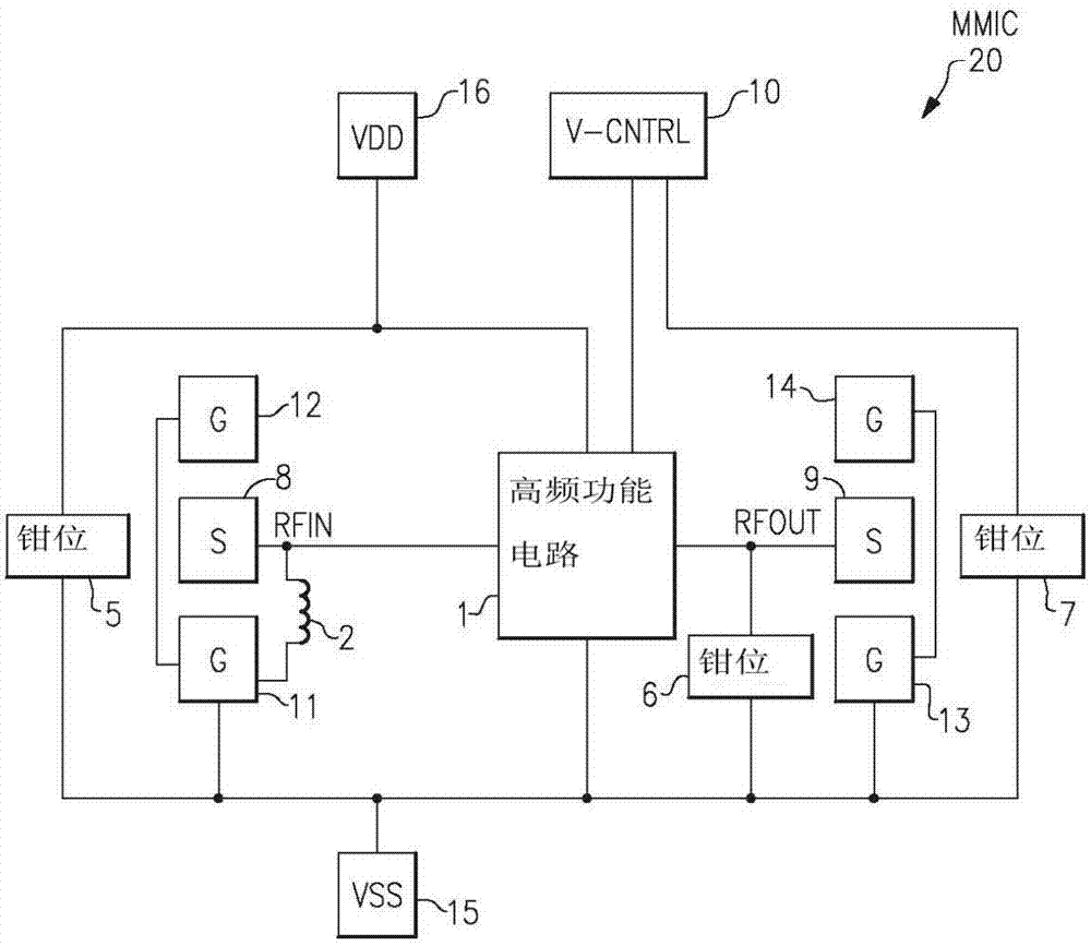
[0021] To help ensure that electronic systems are reliable, manufacturers can test electronic systems under defined stress conditions, which can be described by standards set by various organizations, such as the Joint Electron Device Engineering Council (JEDEC), the International Electrotechnical Society Committee ( IEC) and / or the International Organization for Standardization (ISO). Standards can cover a wide range of transient overstress events, including electrostatic discharge (ESD) events and / or electrical overstress (EOS) events. For example, a monolithic microwave integrated circuit (MMIC) m...


PUM


Abstract

Disclosed are an apparatus and method for transient overstress protection in compound semiconductor circuit applications. An apparatus and methods for compound semiconductor protection clamps are provided herein. In certain configurations, a compound semiconductor protection clamp includes a resistor-capacitor (RC) trigger network and a metal-semiconductor field effect transistor (MESFET) clamp. The RC trigger network detects when an ESD/EOS event is present between a first node and a second node, and activates the MESFET clamp in response to detecting the ESD/EOS event. When the MESFET clamp is activated, the MESFET clamp provides a low impedance path between the first and second nodes, thereby providing ESD/EOS protection. When deactivated, the MESFET clamp provides high impedance between the first and second nodes, and thus operates with low leakage current and small static power dissipation.

Description

technical field [0001] Embodiments of the present invention relate to electronic systems, and more particularly, to compound semiconductor protection devices. Background technique [0002] Electronic circuits can be exposed to transient overstress events or relatively short duration electrical signals with rapidly changing voltages and high power. Transient overstress events include electrostatic discharge / electrical overload (ESD / EOS) events, such as those caused by the sudden release of electrical charge from an object or person into an electronic circuit. Transient overstress events can damage integrated circuits (ICs) due to overvoltage conditions and / or high power dissipation levels over a relatively small area of ​​the IC. High power dissipation can increase circuit temperature and can cause a number of problems such as junction damage, metal damage, and / or surface charge buildup. Contents of the invention [0003] In one aspect, a compound semiconductor circuit is...

Claims


Application Information

Patent Timeline
Patent Type & Authority Applications(China)
IPC IPC(8): H01L27/04
CPCH01L27/04H01L27/0285H01L29/1075H01L29/205H01L29/7783H01L29/8124H01L29/872H01L27/0605H01L27/0629
Inventor S·帕萨萨拉希J·A·塞尔瑟多
Owner ANALOG DEVICES INC
Why Eureka
Try Eureka