Stress-tuned planar lighting circuit and method

A circuit, plane light wave technology, applied in the direction of instruments, optical waveguides, light guides, etc., can solve the problems of a large amount of chip occupied area, high cost per chip, etc., and achieve the effect of cheap PLC chips, low light loss, and improved mechanical coupling.

Active Publication Date: 2020-06-19
LIONIX INT BV
View PDF11 Cites 0 Cited by
  • Summary
  • Abstract
  • Description
  • Claims
  • Application Information

AI Technical Summary

Problems solved by technology

[0018] Therefore, PLCs based on low-contrast waveguides require a large chip footprint for any significant function, which results in a high cost per chip

Method used


Image

  • Stress-tuned planar lighting circuit and method
  • Stress-tuned planar lighting circuit and method
  • Stress-tuned planar lighting circuit and method

Examples


Embodiment Construction

[0050] For the purposes of this specification, including the appended claims, the terms "disposed on" or "formed on" are defined as "present on" an underlying material or layer, or in direct physical contact therewith or by means of one or more middle layer. For example, if a material is described as being "deployed (or grown)" on a substrate, this can mean that either (1) the material is in intimate contact with the substrate; or (2) the material is in contact with one or more layers already present on the substrate touch. It should be noted that a conformal layer is considered to be deployed on each surface of the structure with which it conforms.

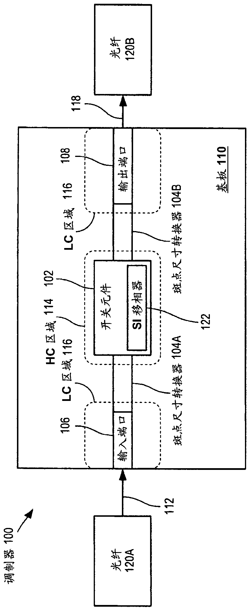
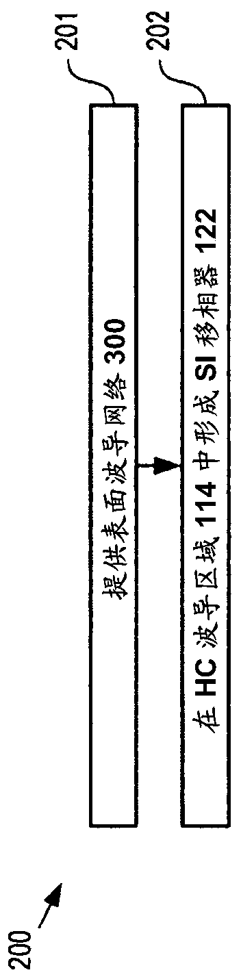
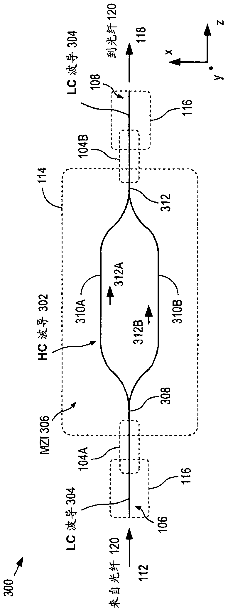
[0051] This case is a continuation-in-part of US Patent Application Serial No. 14 / 051715, entitled "Surface Waveguide Having a Tapered Region and Method of Forming" (hereinafter "parent case"), which is hereby incorporated by reference in its entirety. As discussed in the parent case, the use of waveguide taper-based spot size ...


PUM

PropertyMeasurementUnit
thicknessaaaaaaaaaa
thicknessaaaaaaaaaa
thicknessaaaaaaaaaa

Abstract

A planar lightwave circuit is disclosed that is capable of optical coupling to external devices with low optical loss, while also providing low power functional control of optical signals propagating through a PLC. The PLC includes a high-contrast waveguide region in which stress-induced (SI) phase shifters are formed, enabling it to control the phase of an optical signal. The high-contrast waveguide region is optically coupled to the low-contrast waveguide region via the spot size converter, thereby enabling optical coupling to off-chip devices with low optical losses. Forming the SI phase shifter in the high-contrast waveguide region enables improved responsiveness and phase control, reduced voltage, and a smaller required chip footprint. Thus, the present invention enables a lower cost and higher performance PLC system.

Description

[0001] Cross References to Related Applications [0002] This case is a continuation-in-part of co-pending U.S. Patent Application Serial No. 14 / 051715 (Attorney Docket: 142-024US1) filed on October 11, 2013, which is required to be filed on October 11, 2012 Priority of U.S. Provisional Patent Application Serial No. 61 / 712,587 (Attorney Docket: 142-024PR1), each of which is hereby incorporated by reference. [0003] Furthermore, the underlying concepts (but not necessarily the language) of the following cases are hereby incorporated by reference: [0004] (1) US Patent 7,146,087 issued on December 5, 2006; [0005] (2) U.S. Patent Application Serial No. 14 / 321,138; and [0006] (3) US Patent 7,142,759 issued on November 28, 2006. [0007] In the event of any language inconsistency or inconsistency between this application and one or more cases in this case that have been incorporated by reference that may affect the interpretation of the scope of protection, the scope of prot...

Claims


Application Information

Patent Timeline
Patent Type & Authority Patents(China)
IPC IPC(8): G02F1/025G02F1/225G02B6/122G02B6/132G02B6/14
CPCG02B6/122G02B6/132G02B6/14G02F1/025G02F1/225G02F1/2257G02B6/12007G02B6/1223G02B6/125G02F1/0134G02B6/1228
Inventor R·G·黑德曼A·雷恩斯
Owner LIONIX INT BV
Why Eureka
Try Eureka