Thin film transistor and its manufacturing method, array substrate, display device

A thin-film transistor and array substrate technology, which is applied in the display field, can solve problems such as the deviation of the volt-ampere characteristic curve and affect the normal operation of the thin-film transistor, so as to reduce the degree of deviation of the volt-ampere characteristic curve, reduce the amount of light, and weaken the influence degree of effect

Active Publication Date: 2020-03-13
BOE TECH GRP CO LTD +1
View PDF3 Cites 0 Cited by
  • Summary
  • Abstract
  • Description
  • Claims
  • Application Information

AI Technical Summary

Problems solved by technology

[0005] In order to solve the problem that the volt-ampere characteristic curve of the active layer pattern will shift and affect the normal operation of the thin film transistor, the application provides a thin film transistor and its manufacturing method, an array substrate, and a display device

Method used


Image

  • Thin film transistor and its manufacturing method, array substrate, display device
  • Thin film transistor and its manufacturing method, array substrate, display device
  • Thin film transistor and its manufacturing method, array substrate, display device

Examples


Embodiment Construction

[0081] In order to make the purpose, technical solution and advantages of the present application clearer, the implementation manners of the present application will be further described in detail below in conjunction with the accompanying drawings.

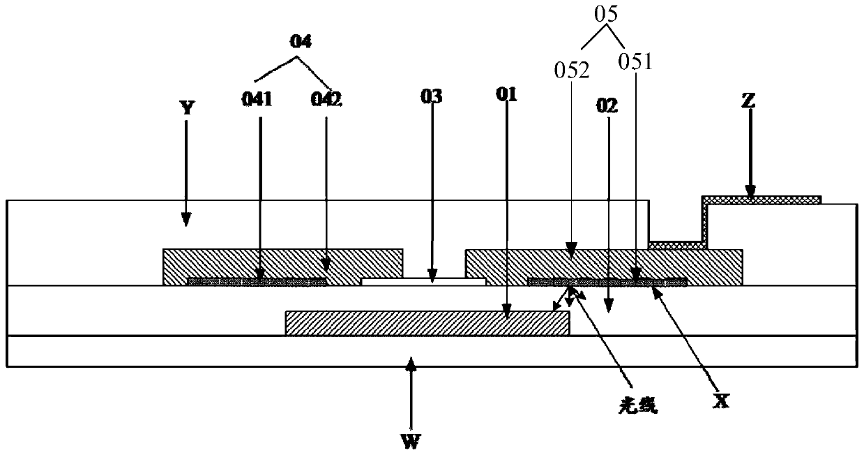
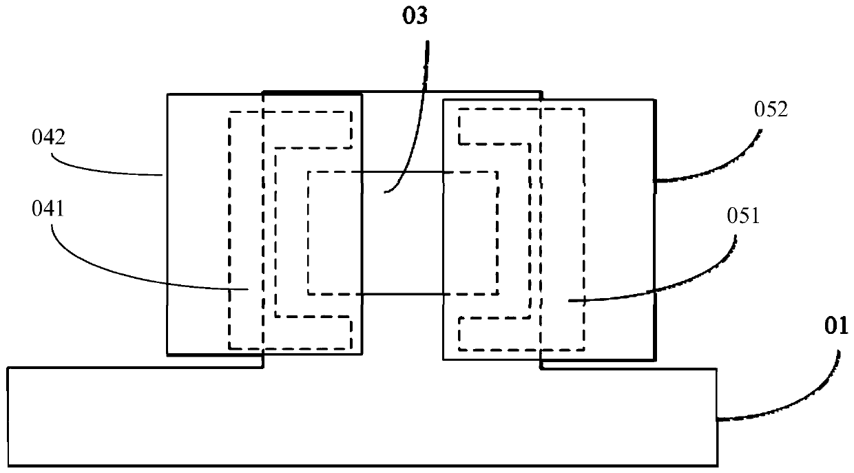
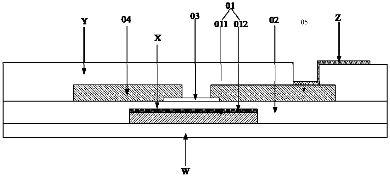
[0082] figure 1 A schematic structural diagram of a thin film transistor provided in an embodiment of the present invention, such as figure 1 As shown, the thin film transistor may include: a gate pattern 01 , a gate insulating layer 02 , an active layer pattern 03 , a source pattern 04 and a drain pattern 05 stacked in sequence.

[0083] Among the surface facing the gate insulating layer 02 in the source pattern 04, the surface facing the gate insulating layer 02 in the drain pattern 05, and the surface facing the gate insulating layer 02 in the gate pattern 01, there is at least one target surface X, and the target surface X The light incident on the target surface can be diffusely reflected to prevent part of the light from e...


PUM


Abstract

The application discloses a thin film transistor, a manufacturing method thereof, an array substrate, and a display device, and belongs to the field of display technology. The thin film transistor includes: a gate pattern, a gate insulating layer, an active layer pattern, a source pattern, and a drain pattern stacked in sequence, the surface of the source pattern facing the gate insulating layer, the surface of the drain pattern facing the gate insulating layer, and Among the surfaces of the gate pattern facing the gate insulating layer, at least one surface is a target surface, and the target surface can diffusely reflect light incident on the target surface, so as to prevent part of the light from entering the active layer pattern. This application solves the problem that the volt-ampere characteristic curve of the active layer pattern will shift, which affects the normal operation of the thin film transistor, and weakens the influence of the target light on the normal operation of the thin film transistor. This application is used in a display device.

Description

technical field [0001] The present application relates to the field of display technology, in particular to a thin film transistor and a manufacturing method thereof, an array substrate, and a display device. Background technique [0002] The array substrate in the display device includes: a base substrate and a plurality of pixel units arranged in an array arranged on one side of the base substrate, each pixel unit may include a thin film transistor, a pixel electrode, a common electrode and a liquid crystal. [0003] In related technologies, different voltages are usually input to pixel electrodes through thin film transistors, thereby changing the degree of deflection of liquid crystals, adjusting the light transmittance of pixel units, and then realizing the function of the display device to display images. Exemplarily, the thin film transistor may include: a gate pattern, a gate insulating layer, an active layer pattern, and a source-drain pattern stacked on the base su...

Claims


Application Information

Patent Timeline
Patent Type & Authority Patents(China)
IPC IPC(8): H01L29/786H01L21/34
CPCH01L29/66969H01L29/78633H01L29/7869H01L21/465H01L21/02565H01L21/467H01L27/1225H01L27/127H01L27/1288
Inventor 操彬彬王超孙林
Owner BOE TECH GRP CO LTD
Why Eureka
Try Eureka