Array substrate, display panel, display device and array substrate manufacturing method

A technology for an array substrate and a display area, which is applied in the fields of array substrate, display device and array substrate fabrication, and display panel, can solve the problems of unfavorable narrow frame of display panel, large area of ​​pressure sensor, etc., and achieves increased square resistance, small area, The effect of reducing interference

Active Publication Date: 2017-09-29
SHANGHAI TIANMA MICRO ELECTRONICS CO LTD
View PDF4 Cites 10 Cited by
  • Summary
  • Abstract
  • Description
  • Claims
  • Application Information

AI Technical Summary

Problems solved by technology

[0004] In the prior art, the pressure sensor is generally arranged in the non-display area of ​​the touch display panel, but the area of ​​the pressure sensor is relatively large, which is not conducive to narrowing the frame of the display panel.

Method used


Image

  • Array substrate, display panel, display device and array substrate manufacturing method
  • Array substrate, display panel, display device and array substrate manufacturing method
  • Array substrate, display panel, display device and array substrate manufacturing method

Examples


Embodiment Construction

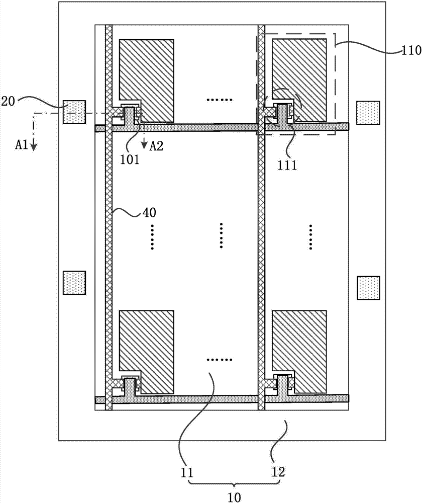
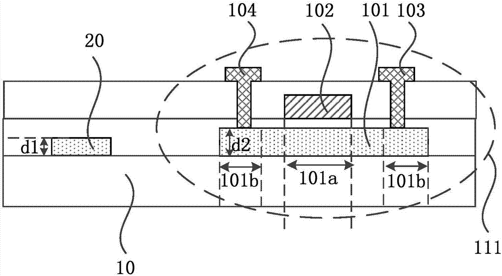
[0035] The present invention will be further described in detail below in conjunction with the accompanying drawings and embodiments. It should be understood that the specific embodiments described here are only used to explain the present invention, but not to limit the present invention. In addition, it should be noted that, for the convenience of description, only some structures related to the present invention are shown in the drawings but not all structures.

[0036] This embodiment provides an array substrate, Figure 1a is a schematic diagram of an array substrate provided by an embodiment of the present invention, Figure 1b is a schematic cross-sectional view of the array substrate along the section line A1-A2, refer to Figure 1a and Figure 1b , the array substrate includes:

[0037] A base substrate 10, the base substrate 10 includes a display area 11 and a non-display area 12 surrounding the display area 11, the display area 11 of the base substrate 10 is provi...


PUM


Abstract

The embodiment of the invention discloses an array substrate, a display panel, a display device and an array substrate manufacturing method. The array substrate comprises a substrate, including a display area and a non-display area surrounding the display area, and at least one pressure sensor. The display area of the substrate is provided with a plurality of pixel units including thin-film transistors. The at least one pressure sensor is located in the non-display area of the substrate, is disposed in the same layer as the active layer of the corresponding thin-film transistor and is fabricated by using the same material as the active layer. The active layer comprises a channel region and a heavily doped region. The square resistance of the pressure sensor is greater than the square resistance of the heavily doped region of the active layer. The area of the pressure sensor is reduced.

Description

technical field [0001] Embodiments of the present invention relate to display technologies, and in particular to an array substrate, a display panel, a display device, and a method for manufacturing the array substrate. Background technique [0002] At present, as an information input tool, a display panel with a touch function is widely used in various display products such as mobile phones, tablet computers, and information inquiry machines in halls of public places. In this way, the user can operate the electronic device only by touching the sign on the touch display panel with his fingers, which eliminates the user's dependence on other input devices (such as keyboard and mouse), and makes human-computer interaction easier. [0003] In order to better meet user needs, a pressure sensor for detecting the touch pressure when the user touches the touch display panel is usually provided in the touch display panel, so that it can not only collect touch position information, b...

Claims


Application Information

Patent Timeline
Patent Type & Authority Applications(China)
IPC IPC(8): H01L27/12H01L21/77G06F3/041
CPCG06F3/0414H01L27/1255H01L27/1259G06F2203/04103G06F2203/04105G06F2203/04106H01L29/78696H01L27/1244H01L27/1288G06F3/0412G06F3/04142G02F1/13338G06F3/04897H01L27/124H01L29/42384
Inventor 周志伟姚绮君卢峰刘亮慎言卞华锋蔡中兰
Owner SHANGHAI TIANMA MICRO ELECTRONICS CO LTD
Why Eureka
Try Eureka