Full-color cholesteric liquid crystal electronic paper
A cholesteric liquid crystal, full-color technology, applied in the field of electronic paper, can solve the problems of easy mechanical external force, increased lead resistance, and increased electrode square resistance, etc., to reduce the overall reflectivity, reduce thickness, and increase transparency. excessive effect
- Summary
- Abstract
- Description
- Claims
- Application Information
AI Technical Summary
Problems solved by technology
Method used
Image
Examples
Embodiment 1
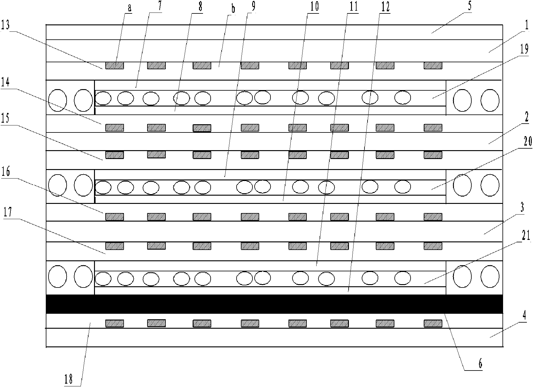
[0045] Such as figure 1As shown, the overall structure of the full-color cholesteric liquid crystal electronic paper provided in this embodiment is three liquid crystal cells formed by stacking the first substrate 1, the second substrate 2, the third substrate 3, and the fourth substrate 4. There are liquid crystal layers capable of reflecting red, green, and blue light, that is, the first liquid crystal layer 19, the second liquid crystal layer 20, and the third liquid crystal layer 21; the first vertical alignment film 7 and the second vertical alignment film 8 are respectively connected with the first vertical alignment film A liquid crystal layer 19 is adjacent; the third vertical alignment film 9 and the fourth vertical alignment film 10 are respectively adjacent to the second liquid crystal layer 20; the fifth vertical alignment film 11 and the sixth vertical alignment film 12 are respectively adjacent to the third liquid crystal layer 21 adjacent.
[0046] The second s...
Embodiment 2
[0054] Figure 4 It is a schematic structural diagram of the full-color cholesteric liquid crystal electronic paper provided in this embodiment. In order to avoid redundant description, the differences from Embodiment 1 are mainly described here.
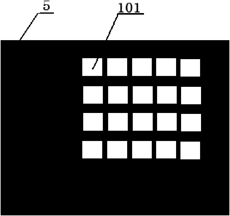
[0055] The light-shielding layer 5' of the full-color cholesteric liquid crystal electronic paper provided in this embodiment is coated on the lower surface of the first substrate electrode 13' and is adjacent to the front first vertical alignment film 7'. The light-shielding layer 5' of this embodiment The structure is the same as that of the first embodiment, the light-shielding layer 5 ′ only covers the non-display area of the first substrate 1 ′, and does not cover the display area, and the thickness of the light-shielding layer 5 ′ is 0.1 μm.
[0056] The light absorbing layer 6' of this embodiment is attached to the sixth substrate electrode 18' and adjacent to the fourth substrate 4'.
[0057] The first substrate electrode...
Embodiment 3
[0059] Such as Image 6 As shown, the difference between the cholesteric liquid crystal electronic paper provided in this embodiment and the second embodiment is that the light-shielding layer 5″ is coated on the surface of the first substrate electrode 13″ and is adjacent to the first substrate 1″. The light-shielding layer of this embodiment The structure of 5" is the same as that of the second embodiment, the light-shielding layer 5" only covers the non-display area of the first substrate 1", and the thickness of the light-shielding layer 5" is 10um.
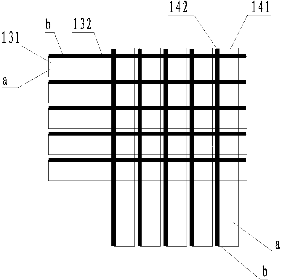
[0060] It should be noted that the thickness of the light-shielding layer of the full-color cholesteric liquid crystal electronic paper provided by the present invention is in the range of 0.1 um to 10 um, the square resistance of the transparent electrode should be greater than 150 Ω / □, and the thickness of the metal electrode is 50 angstroms to 3000 Å. Within the range of angstroms, the material of the metal electrode can...
PUM
| Property | Measurement | Unit |
|---|---|---|
| thickness | aaaaa | aaaaa |
| thickness | aaaaa | aaaaa |
| thickness | aaaaa | aaaaa |
Abstract
Description
Claims
Application Information


