A display device and its manufacturing method
A technology for display devices and display areas, which is applied in semiconductor devices, electric solid state devices, electrical components, etc., and can solve problems such as naked-eye 3D complexity.
- Summary
- Abstract
- Description
- Claims
- Application Information
AI Technical Summary
Problems solved by technology
Method used
Image
Examples
Embodiment 1
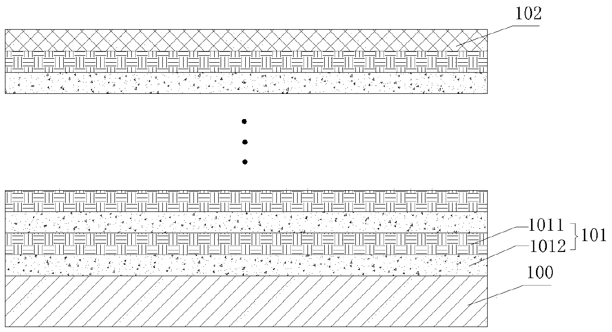
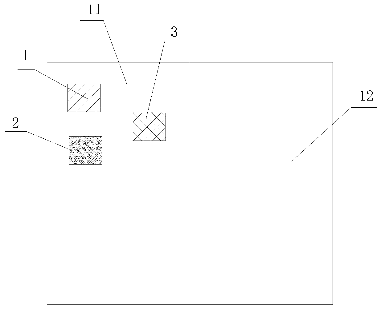
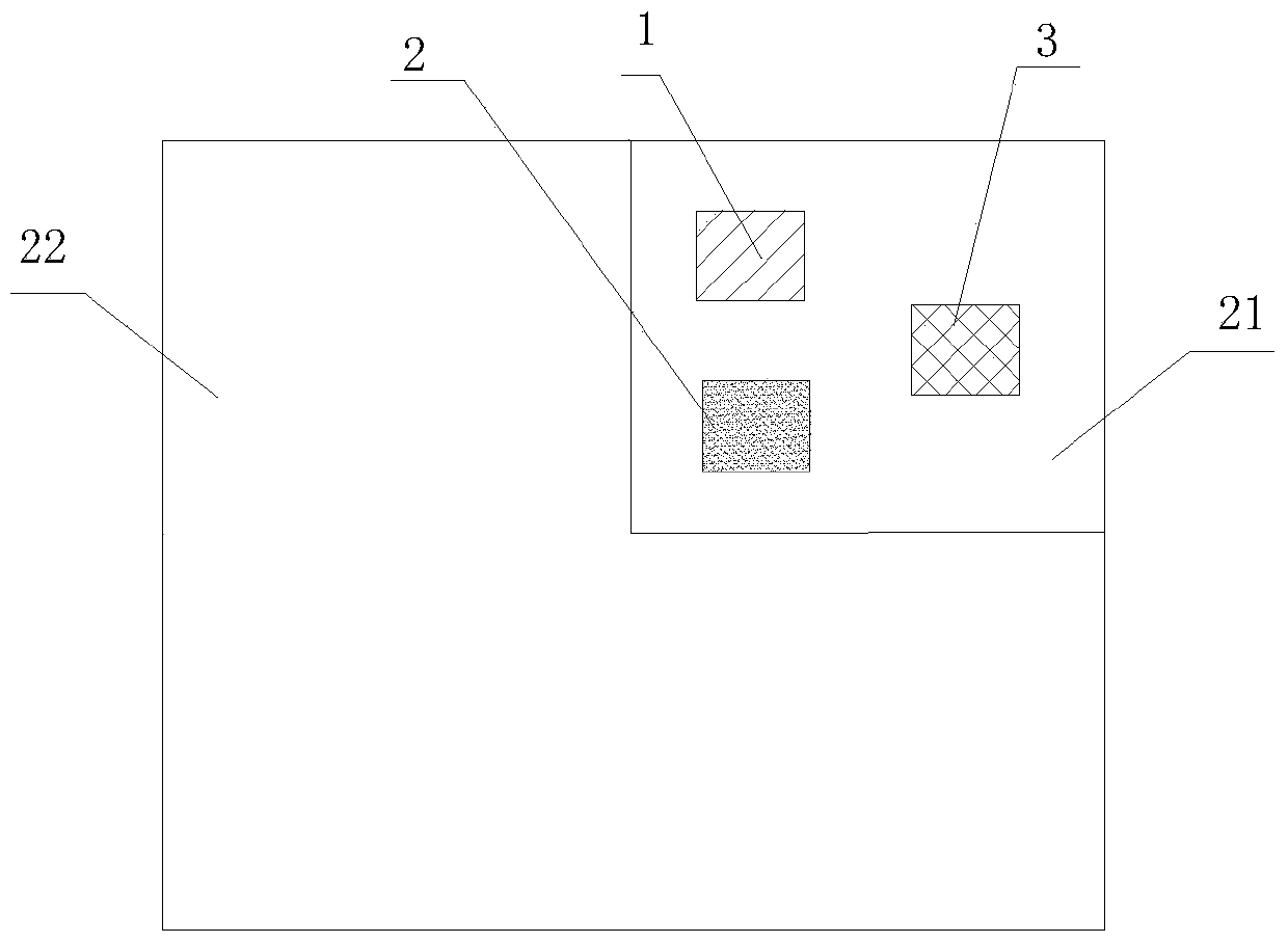
[0027] Such as figure 1 As shown, this embodiment relates to a display device, specifically, the display device includes: a substrate 100 and N-layer organic light emitting devices 101 stacked in sequence on the substrate 100 (that is, all the organic light emitting devices 101 are vertically overlapped), and each layer of organic light emitting devices 101 in the N layers of organic light emitting devices 101 includes a light-transmitting region (the light-transmitting region is not provided with pixels at all) and a display region. In an embodiment of the present invention, each layer of organic light-emitting The light-emitting device 101 includes only one organic light-emitting device; wherein, the display area of the organic light-emitting device 101 in the Mth layer (the organic light-emitting device 101 in any layer except the organic light-emitting device 101 located on the uppermost layer) is the same as the organic light-emitting device in the N-th layer. At least ...
Embodiment 2
[0044] Such as Figure 5 As shown, this embodiment is roughly the same as Embodiment 1, and the display device includes a substrate 200, an N-layer organic light emitting device, and a cover glass 203; the only difference is that each layer of organic light emitting devices in this embodiment includes two organic light emitting devices Devices 201, 202; of course, each layer of organic light emitting devices may include two organic light emitting devices 201, 202 as shown in the figure, or may include three or more organic light emitting devices, as long as the organic light emitting device of the Mth layer The display area (an organic light-emitting device in any layer other than the organic light-emitting device located in the uppermost layer) and at least part of the light-transmitting area of the organic light-emitting device in the Nth layer (the organic light-emitting device located in the uppermost layer) overlap each other, and each layer The pictures displayed in th...
Embodiment 3
[0046] Such as Image 6 As shown, this embodiment relates to a method for manufacturing a display device. Specifically, the method includes:
[0047] In step S1, a substrate is provided, which may be a flexible or rigid substrate, wherein the flexible manufacturing process is more difficult than the rigid one, but this does not affect the purpose of the present invention.
[0048] Step S2, preparing N-layer organic light-emitting devices on the substrate; wherein, each N-layer organic light-emitting device includes a light-transmitting area and a display area, and the display area of the M-layer organic light-emitting device is at least the same as the N-layer organic light-emitting device. Part of the light-transmitting regions overlap each other, and N and M are both natural numbers, and M
[0049] In a preferred embodiment of the present invention, the steps of preparing each layer of the organic light-emitting device include:
[0050] forming a driving element, opti...
PUM
 Abstract
Description
Claims
Application Information
 - R&D
- Intellectual Property
- Life Sciences
- Materials
- Tech Scout
- Unparalleled Data Quality
- Higher Quality Content
- 60% Fewer Hallucinations
Browse by: Latest US Patents, China's latest patents, Technical Efficacy Thesaurus, Application Domain, Technology Topic, Popular Technical Reports.
© 2025 PatSnap. All rights reserved.Legal|Privacy policy|Modern Slavery Act Transparency Statement|Sitemap|About US| Contact US: help@patsnap.com


